Category: Packaging & Testing
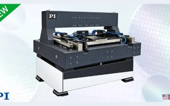
October 27, 2026 · 2 mins read
Physik Instrumente (PI) has unveiled the A-323 planar air bearing scanner at SEMICON West 2026, introducing a high-dynamic precision motion platform engineered for semiconductor […]
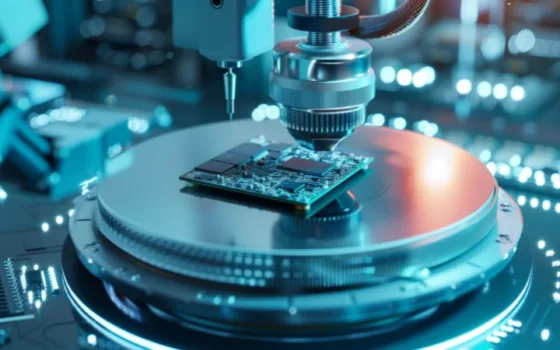
October 24, 2026 · 2 mins read
Madhya Pradesh has secured investment proposals valued at approximately ₹5,800 crore across the semiconductor and advanced technology sectors during an industry summit in Indore. […]
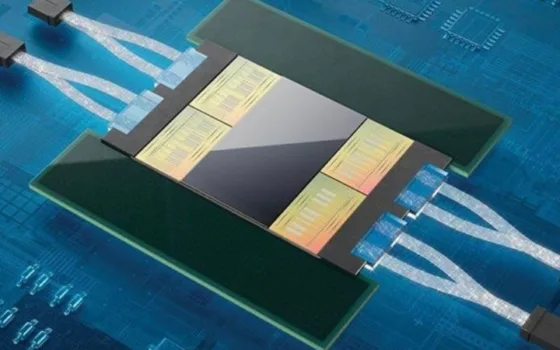
October 22, 2026 · 2 mins read
A four-company joint research and development consortium led by NTT Innovative Devices Corporation has been selected under Japan’s New Energy and Industrial Technology Development […]
October 22, 2026 · 2 mins read
Samsung Electro-Mechanics has entered into a strategic business partnership with NVIDIA to expand dedicated manufacturing capacity for Ajinomoto Build-up Film (ABF) package substrates, aiming […]
October 21, 2026 · 2 mins read
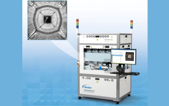
The SonoFlex Acoustic System from Nordson Test & Inspection has been named the recipient of the Best of West award at SEMICON West 2026. […]
October 21, 2026 · 8 mins read
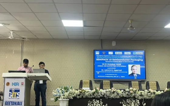
Introduction The Department of Electronics and Communication Engineering (ECE), Geetanjali Institute of Technical Studies (GITS), Udaipur, successfully organized SEMIPACK 1.0 – Semiconductor Packaging International […]
October 21, 2026 · 4 mins read
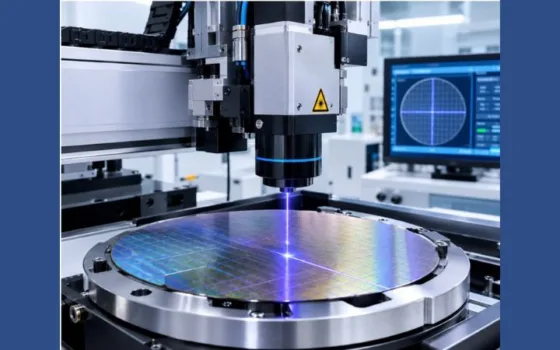
Market Summary According to latest research by Growth Market Reports, the global semiconductor laser scribing equipment market size reached USD 1.64 billion in 2025, […]
October 19, 2026 · 2 mins read
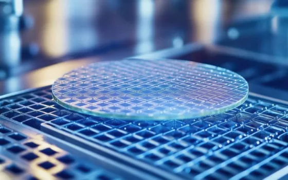
Keysight Technologies, the University of Glasgow, the UK’s National Physical Laboratory (NPL), and Taiwan-based probing specialist MPI Corporation have jointly demonstrated continuous on-wafer characterization […]
October 19, 2026 · 2 mins read
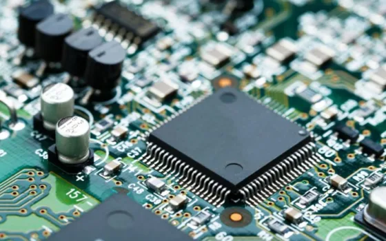
The Madhya Pradesh government will host the two-day Madhya Pradesh Semiconductor Summit 2026 at the Brilliant Convention Centre in Indore on October 23 and […]
October 18, 2026 · 2 mins read
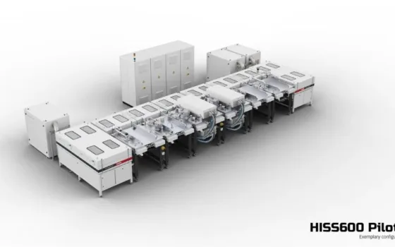
VON ARDENNE has expanded its semiconductor physical vapor deposition portfolio into panel-level packaging (PLP), deploying high-power impulse magnetron sputtering (HiPIMS) technology on its proprietary […]
