Market Summary
According to latest research by Growth Market Reports, the global semiconductor laser scribing equipment market size reached USD 1.64 billion in 2025, reflecting robust expansion driven by the increasing adoption of advanced manufacturing technologies across the semiconductor industry. The market is projected to grow at a CAGR of 7.9% from 2026 to 2034, reaching a forecasted value of USD 3.28 billion by 2034. The primary growth factor fueling this surge is the escalating demand for high-precision, high-throughput laser scribing solutions across semiconductor manufacturing, photovoltaics, and electronics sectors, as manufacturers strive to improve yield, reduce defects, and increase production efficiency.
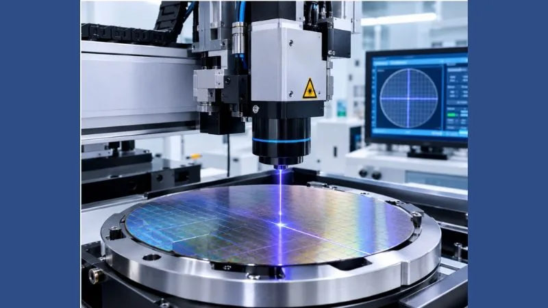
The Semiconductor Laser Scribing Equipment Market is gaining importance as semiconductor manufacturers seek precise, efficient, and reliable techniques for processing wafers and separating individual chips. Laser scribing uses focused laser energy to create narrow grooves or defined cutting paths in semiconductor materials. This process supports controlled material removal while helping manufacturers manage damage, improve production consistency, and optimize fabrication workflows.
Key Drivers
Rising Demand for Advanced Semiconductor Devices
The growing adoption of semiconductors across consumer electronics, automotive systems, telecommunications, industrial automation, and computing is strengthening demand for advanced manufacturing equipment. Modern electronic products require compact chips with improved performance and reliability. Laser scribing helps manufacturers create precise separation paths and process delicate materials according to specific production requirements.
The expansion of artificial intelligence hardware, electric vehicles, connected devices, and high-performance computing is also encouraging semiconductor producers to improve manufacturing capabilities. As chip designs evolve, equipment capable of delivering repeatable and controlled processing is becoming increasingly relevant.
Increasing Focus on Manufacturing Precision
Traditional mechanical processing methods can introduce stress, chipping, or material damage in certain semiconductor applications. Laser-based techniques offer an alternative by enabling localized energy delivery and fine control over scribing parameters. Depending on the material and process configuration, these systems can support narrower grooves and improved edge quality.
Manufacturers are increasingly prioritizing production consistency and yield optimization. Equipment that reduces material loss and supports reliable processing can contribute to more efficient manufacturing operations, particularly when handling fragile wafers or advanced semiconductor structures.
Challenges
High Equipment and Integration Costs
Advanced laser scribing systems require specialized laser sources, precision optics, motion-control components, imaging systems, and process-management software. These requirements can increase initial investment and make adoption difficult for smaller semiconductor manufacturers. Integration with existing production lines may also require equipment modifications, operator training, and extensive process validation.
Technical Complexity and Material Compatibility
Different semiconductor materials respond differently to laser wavelengths, pulse durations, and energy levels. Selecting suitable operating parameters is essential to minimize thermal damage, debris, microcracks, and other defects. Manufacturers must continuously refine their processes to achieve consistent results across diverse wafer thicknesses, material compositions, and device structures.
Emerging Opportunities and Technological Advancements
Ultrafast Lasers and Advanced Processing Methods
Developments in picosecond and femtosecond laser technology are creating opportunities for more controlled material processing. These ultrafast systems can limit heat transfer to surrounding areas under appropriate process conditions, making them attractive for sensitive semiconductor applications. Innovations in beam shaping, wavelength selection, and laser pulse control are also helping equipment developers address increasingly demanding production requirements.
Automation and Intelligent Process Monitoring
Automated equipment is becoming increasingly valuable as semiconductor manufacturers pursue consistent quality and higher production throughput. Machine vision, precision positioning, real-time monitoring, and automated inspection can help identify process deviations and reduce manual intervention. Integration with factory automation platforms can also improve production traceability and equipment utilization.
These capabilities create opportunities for manufacturers to develop flexible systems that support multiple product specifications and shorten changeover times. Predictive maintenance and data-driven process optimization may further improve equipment reliability and operational efficiency.
Competitive Landscape
DISCO Corporation
Han’s Laser Technology Industry Group Co., Ltd.
Coherent Corp.
IPG Photonics Corporation
3D-Micromac AG
Lumentum Holdings Inc.
MKS Instruments, Inc.
Oxford Lasers Ltd.
InnoLas Solutions GmbH
Synova SA
Future Outlook
The Semiconductor Laser Scribing Equipment Market is positioned for continued development as semiconductor manufacturers invest in advanced processing technologies and increasingly sophisticated electronic components. Growth opportunities are expected to emerge from wafer miniaturization, advanced packaging, compound semiconductor applications, and automation. Continued improvements in laser precision, process monitoring, and equipment flexibility will remain important as manufacturers seek to improve yield, reduce material waste, and meet evolving semiconductor production requirements.
Source: Growth Market Reports