A four-company joint research and development consortium led by NTT Innovative Devices Corporation has been selected under Japan’s New Energy and Industrial Technology Development Organization (NEDO) program to establish volume manufacturing technologies for photonics-electronics convergence (PEC) devices. The initiative operates under NEDO’s Research and Development Project of the Enhanced Infrastructures for Post-5G Information and Communication Systems / Development of Manufacturing Technologies for Advanced Semiconductors, with NTT serving as project advisor.
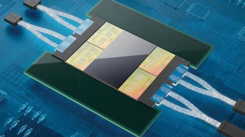
The accelerated buildout of generative artificial intelligence and high-performance computing (HPC) clusters is creating severe interconnect bottlenecks across hyperscale data centres. As computing nodes process massive parallel datasets, conventional electrical chip-to-chip copper interconnects face escalating latency, signal attenuation, and unsustainable thermal dissipation. Photonics-electronics convergence bridges this performance divide by replacing lossy copper wiring with optical signaling, delivering multi-terabit bandwidth at substantially lower power consumption.
Under the joint initiative, NTT Innovative Devices, Japan Semiconductor Corporation, Furukawa Electric Co., Ltd., and Shinko Electric Industries Co., Ltd. will combine their respective capabilities across silicon photonics, optical semiconductors, high-density packaging, optical interconnects, and high-volume backend assembly. The team aims to build and qualify a dedicated pilot production line designed to validate commercial fabrication recipes, targeting more than a tenfold productivity increase over current laboratory and prototype-scale processes.
The project builds upon ongoing R&D conducted since fiscal year 2023, where NTT has spearheaded optical chiplet packaging frameworks that use light to interconnect semiconductor dies and organic package substrates. NTT’s advisory role within the new phase focuses on aligning multi-vendor technical interfaces, cultivating cross-industry collaboration, and anchoring a domestic supply chain for scalable PEC integration.
For the semiconductor industry, transitioning optical chiplets from boutique assembly into repeatable, high-volume advanced packaging lines is a prerequisite for next-generation AI architectures. Monolithic lithography scaling alone can no longer satisfy data transfer requirements between accelerators and memory tiers. By establishing industrialized pilot lines and standardizing multi-die optical packaging protocols, the Japanese consortium is addressing the foundational manufacturing barriers required to make co-packaged optics and photonic interconnects commercially viable for global AI hardware infrastructure.