Introduction
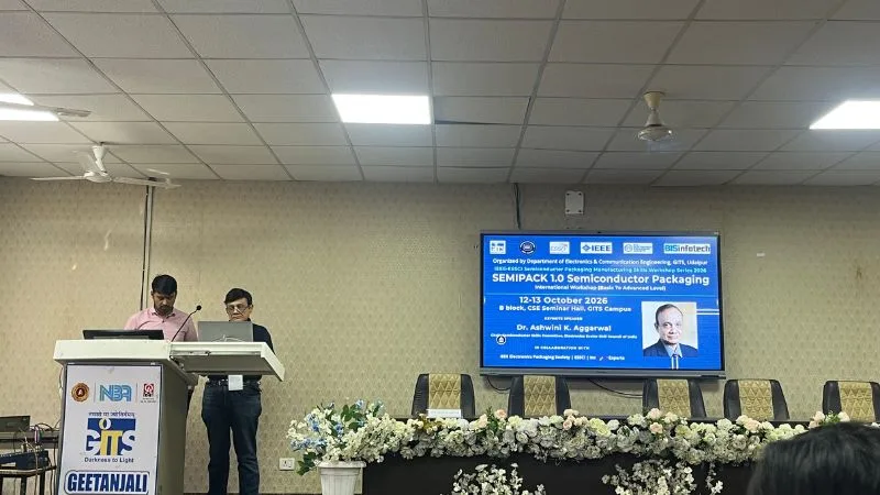
The Department of Electronics and Communication Engineering (ECE), Geetanjali Institute of Technical Studies (GITS), Udaipur, successfully organized SEMIPACK 1.0 – Semiconductor Packaging International Workshop (Basic to Advanced) on 12–13 October 2026. Funded by IEEE, the workshop was conducted under the IEEE Electronics Packaging Society (EPS) Student Branch Chapter of GITS.
The two-day event covered conventional and advanced semiconductor packaging, heterogeneous integration, optoelectronics, quantum technologies, and semiconductor manufacturing.
With over 180 registrations, the workshop welcomed participants from GITS, Techno NJR, Mewar University, and CTAE, providing a platform for technical learning and interaction with academic and industry experts through in-person and virtual sessions.
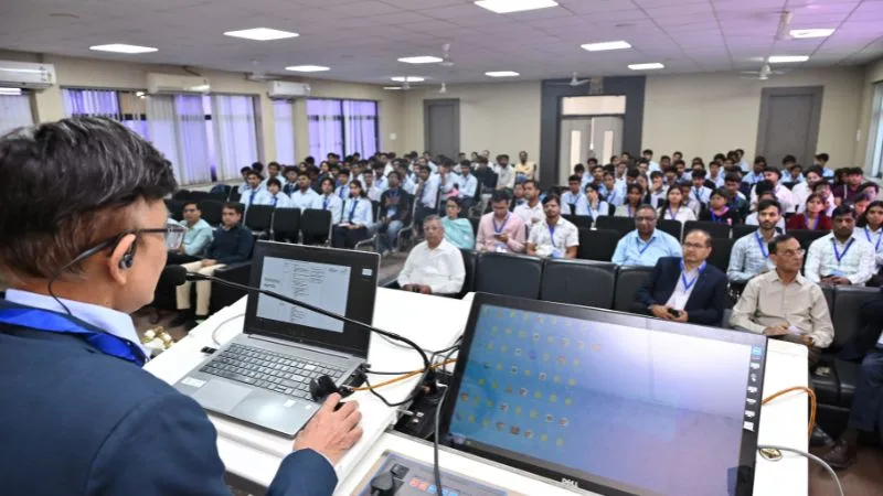
Day One – 12 October 2026
Inaugural Ceremony
The first day commenced at approximately 9:45 AM following the registration of participants. The arrival of the keynote speaker, Dr. Ashwini K. Aggarwal, marked the beginning of the programme. The inaugural ceremony included the ceremonial lamp lighting, felicitation of the dignitaries, and an address by the Director of GITS, followed by an address by Shri P. K. Jain. The inaugural proceedings formally set the stage for the commencement of the technical workshop.
Session 1: Skilling India on Semiconductor Manufacturing – ESSCI Programme and India’s Semiconductor Landscape
Dr. Ashwini K. Aggarwal introduced participants to the broader semiconductor manufacturing ecosystem in India, highlighting the role of the Electronics Sector Skills Council of India (ESSCI) in developing a skilled workforce for the semiconductor industry.
The session covered the Indian semiconductor market, its growth potential, and the major sectors driving demand, including manufacturing, renewable energy, the digital economy, pharmaceuticals, and infrastructure. The speaker also discussed India’s semiconductor fabrication landscape, the challenges associated with entering this capital-intensive industry, and key roadblocks involving workforce development, infrastructure readiness, and India’s relatively late entry into semiconductor manufacturing.
Further discussions focused on the India Semiconductor Mission (ISM), its policy framework and long-term roadmap, the approved semiconductor projects, and the evolving landscape of outsourced semiconductor assembly and test (OSAT) facilities in India. Projects and organizations discussed included Micron, Tata Electronics, Kaynes Semicon, Semiconductor Laboratory (SCL), and HORIBA, along with the pillars of SEMICON 2.0.
The session provided participants with a broader understanding of India’s ambitions to establish a competitive semiconductor manufacturing ecosystem and strengthen domestic capabilities.
Session 2: Kaynes OSAT Journey
A virtual technical session was delivered by Dr. Wasiuddin, Director–Technical, Kaynes Semiconductors, on the journey of Kaynes in the OSAT domain.
The session introduced participants to the role of OSAT facilities in semiconductor manufacturing and the importance of assembly, packaging, and testing in the semiconductor value chain. It offered an industry-oriented perspective on India’s growing semiconductor packaging ecosystem and the opportunities emerging in domestic semiconductor manufacturing.
Session 3: Anatomy of an Electronics Packaging System
Dr. Ashwini K. Aggarwal subsequently conducted an extensive technical session on the anatomy of an electronics packaging system. The session introduced the fundamentals of semiconductor packaging, package design, different package types, and the distinctions between conventional and advanced packaging technologies.
Participants were guided through the process flow of conventional semiconductor packaging, gaining an understanding of how semiconductor dies are transformed into protected, interconnected, and functional packaged components.
The session also introduced the major job processes involved in a conventional packaging unit, with particular emphasis on wafer dicing. The discussion covered the significance of wafer separation in semiconductor manufacturing and its relationship with subsequent packaging operations.
Post-Lunch Technical Session: Conventional Packaging Unit Job Processes
Following the lunch break, Dr. Aggarwal continued the detailed discussion on conventional packaging processes. The session covered the following topics:
- Lead frames and their role in package interconnection.
- Die attach techniques and their importance in mechanical and thermal integration.
- Wire bonding and electrical interconnection between the die and package.
- Package encapsulation, molding, and sealing for physical and environmental protection.
- Lead finishing, trimming, and solder ball attachment.
- Bumping and bonding processes.
- Substrate materials and their role in package design.
- Underfill materials and their applications in improving package reliability.
- Singulation and the separation of individual packaged devices.
- Assembly and packaging business considerations.
The speaker explained the interdependence of these processes and highlighted their importance in determining the electrical performance, thermal behaviour, manufacturability, and long-term reliability of semiconductor packages.
The session concluded after a tea break, marking the successful completion of Day One. The day provided participants with a strong foundation in semiconductor manufacturing and conventional packaging technologies.
Day Two – 13 October 2026
Recapitulation and Completion of Conventional Packaging
The second day began with a recap of the concepts covered on Day One, helping participants revisit the fundamentals and consolidate their understanding of conventional semiconductor packaging.
The discussion progressed to additional topics, including the semiconductor value chain, interposers, coreless substrates, BGA underfill processes, and the fundamentals of singulation. These topics helped establish a conceptual bridge between conventional packaging methods and more sophisticated approaches used in modern
semiconductor devices.
Session 1: Advanced Packaging
A virtual technical session on Advanced Packaging was delivered by Mr. Nishant Sharma, Indian Institute of Science (IISc), Bengaluru.
The session explored the growing importance of advanced packaging in meeting the performance and integration requirements of modern electronic systems. Key topics included packaging for physical protection of the semiconductor die, encapsulation, heat dissipation, thermal interface materials (TIMs), and the expansion of functionality through innovative packaging approaches.
The discussion also addressed package warpage and flexible printed circuit board (PCB) approaches, highlighting the importance of material selection, mechanical stability, and thermal management in advanced package design.
Session 2: Advanced Packaging – Applied Materials
Following the tea break, participants attended a virtual session by Mr. Nilesh of Applied Materials (AMAT) on advanced packaging.
The session provided an industry-oriented perspective on developments in advanced semiconductor packaging and its relevance to next-generation semiconductor devices. It further strengthened participants’ understanding of the technological developments shaping the future of semiconductor manufacturing and packaging.
Session 3: Photonics and Optoelectronics Packaging
An insightful virtual session on Photonics and Optoelectronics Packaging was delivered by Dr. Rohin Y. of LightSpeed Photonics.
The session introduced participants to photonics packaging and its growing significance in high-speed communication and emerging electronic systems. The speaker discussed the differences between conventional electronic packaging and photonics packaging, along with the distinct integration and packaging considerations associated with optical components.
The session also highlighted the future scope of photonics packaging and its potential role in supporting next-generation communication technologies and high-performance computing systems.
Session 4: Packaging for Quantum Technologies
Dr. Ashwini K. Aggarwal conducted another detailed session on Packaging for Quantum Technologies, introducing participants to the specialized requirements of packaging quantum chips and quantum devices.
The discussion covered the importance of packaging in protecting sensitive quantum components, maintaining suitable operating environments, and ensuring reliable interconnections. Particular emphasis was placed on cryogenic operating conditions and the challenges associated with thermal management, signal integrity, and the physical integration of quantum devices.
The session offered participants an introduction to an emerging area at the intersection
of semiconductor packaging and quantum technology.
Post-Lunch Special Session: LAM SEMulator3D
Following the lunch break, Dr. Aggarwal conducted a special session on LAM SEMulator3D, introducing participants to the use of three-dimensional process modelling and semiconductor process simulation.
The session demonstrated how simulation tools can be used to understand semiconductor fabrication processes and visualize complex three-dimensional structures. It helped participants appreciate the role of virtual process modelling in analysing fabrication steps, understanding process interactions, and supporting semiconductor technology development.
The session provided a practical perspective on the relevance of simulation tools in modern semiconductor engineering and process development.
Valedictory Session and Certificate Distribution
The workshop concluded with a wrap-up session summarizing the major technical insights and learning outcomes from the two-day programme. A formal vote of thanks was delivered, followed by the certificate distribution ceremony to recognize the participation and involvement of attendees.
The contributions of the student organizing committee and the IEEE student chapter members were appreciated for their efforts in coordinating the event, managing registrations, supporting the technical sessions, and ensuring the smooth execution of the programme.
Key Outcomes and Learning
SEMIPACK 1.0 provided participants with a structured introduction to semiconductor packaging, progressing from fundamental conventional packaging processes to advanced and emerging technologies.
The key outcomes of the workshop included:
- Understanding India’s semiconductor ecosystem: Participants gained insights into the India Semiconductor Mission, OSAT facilities, domestic semiconductor projects, and the country’s semiconductor manufacturing ambitions.
- Exposure to conventional packaging: The workshop covered wafer dicing, die attach, wire bonding, encapsulation, substrates, underfills, and singulation.
- Awareness of advanced packaging technologies: Participants explored interposers, advanced substrates, thermal management, warpage, and next-generation packaging approaches.
- Introduction to emerging technologies: Sessions on photonics packaging and quantum technology packaging highlighted specialized packaging requirements and future opportunities.
- Industry–academia interaction: Contributions from industry experts and academic professionals provided diverse perspectives on semiconductor manufacturing, packaging, and process simulation.
- Practical awareness of simulation tools: The LAM SEMulator3D session introduced participants to three-dimensional semiconductor process modelling and its relevance to fabrication technology.
Acknowledgements
The successful organization of SEMIPACK 1.0 was made possible through the support and guidance of Prof. Pradeep C. Garg, Head of the Department of Electronics and Communication Engineering, GITS, whose encouragement and support were instrumental in facilitating the initiative.
The organizers express their sincere gratitude to IEEE for funding the workshop and supporting student-led technical initiatives. Special appreciation is extended to the IEEE EPS Student Branch Chapter and the IEEE SID Student Chapter at GITS for their collaborative efforts and contributions to the event.
The organizing team also extends its gratitude to Dr. Ashwini K. Aggarwal, Dr. Wasiuddin, Mr. Nishant Sharma, Mr. Nilesh, Dr. Rohin Y., and all other speakers and contributors for sharing their knowledge, expertise, and valuable perspectives with the participants.
The participation of students and faculty members from GITS, Techno NJR, Mewar University, CTAE, and other institutions across Udaipur contributed significantly to the success of the workshop.
Conclusion
SEMIPACK 1.0 successfully brought together students, academic professionals, and industry experts for two days of technical learning and knowledge exchange in semiconductor packaging. With more than 180 registrations, the workshop served as a valuable platform for developing awareness of India’s semiconductor manufacturing ecosystem and the technological advancements shaping the future of packaging.
The workshop’s progression from conventional packaging fundamentals to advanced packaging, photonics, quantum technologies, and process simulation enabled participants to appreciate both established industrial practices and emerging areas of research and development.
The positive response from the participants and the appreciation received by the organizing team reflected the effectiveness of the initiative. The event reinforced the importance of industry–academia collaboration and student-led technical activities in preparing aspiring engineers for opportunities in the semiconductor industry.
SEMIPACK 1.0 concluded successfully, marking a meaningful step towards strengthening semiconductor packaging awareness, technical learning, and industry-oriented education at GITS.