Samsung Electro-Mechanics has entered into a strategic business partnership with NVIDIA to expand dedicated manufacturing capacity for Ajinomoto Build-up Film (ABF) package substrates, aiming to fortify global artificial intelligence hardware supply chains. Under the terms of the agreement, the two companies will jointly finance the expansion of production infrastructure across Samsung Electro-Mechanics’ facilities in Sejong and Busan, South Korea.Commercial deliveries of high-density ABF substrates to NVIDIA are scheduled to commence in 2026.
The long-term supply agreement covers advanced package substrates for NVIDIA’s high-performance AI compute chipsets as well as its ultra-fast networking switches deployed in scale-out data center environments. From the initial 2026 ramp, delivery volumes are projected to expand at a double-digit compound annual rate. By 2028, production allocated directly to NVIDIA will represent a significant share of Samsung Electro-Mechanics’ total annual package substrate output, providing NVIDIA with secured backend capacity while alleviating persistent supply chain bottlenecks in high-density packaging.
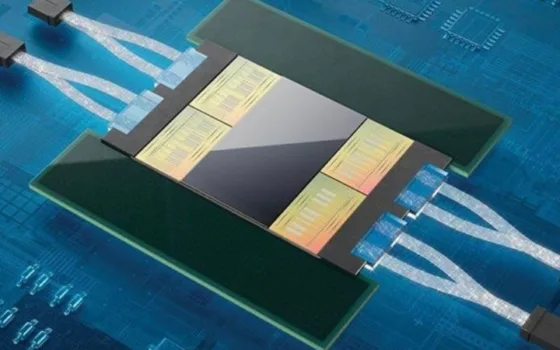
As AI accelerators move toward multi-die modular architectures, package substrates must grow substantially in physical surface area while accommodating complex multi-layer interconnects. Larger substrate form factors introduce acute physical hurdles, including mechanical warpage, localized thermal stress, and signal attenuation across ultra-fine circuit traces. Furthermore, high-power processor clusters require advanced power integrity solutions to suppress switching transients and voltage noise during peak compute cycles. To address these electrical demands, modern advanced packaging flows embed passive components—such as multilayer ceramic capacitors (MLCCs) and high-density silicon capacitors—directly into the substrate core.
Samsung Electro-Mechanics brings proprietary microfabrication capabilities alongside established high-volume MLCC engineering to resolve these packaging yield challenges. Duck-Hyun Chang, President and CEO of Samsung Electro-Mechanics, stated that combining the company’s FC-BGA substrate manufacturing lines with differentiated MLCC technology allows it to deliver stable packaging solutions to support NVIDIA’s platform rollouts. Debora Shoquist, Executive Vice President of Operations at NVIDIA, emphasized that meeting the velocity of the global AI buildout requires expanding substrate manufacturing capacity globally to scale accelerated computing platforms.
For the broader semiconductor industry, the alliance highlights how advanced package substrates have become a strategic choke point in scaling AI hardware. As front-end lithography reaches physical scaling limits, performance gains increasingly rely on backend heterogeneous integration, where large-format ABF substrates bridge advanced silicon dies with system boards. By locking in dedicated, co-invested capacity with Samsung Electro-Mechanics, NVIDIA strengthens its upstream manufacturing resilience against packaging shortages, establishing a stable supply corridor for next-generation computing infrastructure.