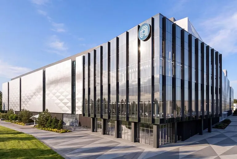
Applied Materials has unveiled its Equipment and Process Innovation and Commercialization (EPIC) Center at its Sunnyvale, California campus, committing approximately $5 billion in capital investment to build the semiconductor industry’s largest collaborative research and development facility. The 600,000-square-foot complex incorporates nearly four acres of advanced cleanroom infrastructure designed to bridge the gap between early materials science, equipment design, and volume manufacturing. The initiative directly targets the escalating structural complexity of leading-edge logic, high-bandwidth memory (HBM), and advanced multi-die packaging required for artificial intelligence workloads.
Historically, microelectronics innovation has followed a serialized development lifecycle: fundamental materials research takes place in research laboratories, tool vendors develop deposition and etch hardware separately, and foundries qualify the resulting recipes across pilot fab lines. This fragmented handoff structure has become a bottleneck as transistor architectures move past sub-2nm nodes and 3D heterogeneous packaging becomes standard. At atomic dimensions, new materials interfaces behave unpredictably, requiring synchronized hardware co-optimization. The EPIC facility replaces this sequential chain with a parallel framework, colocating device makers, subsystem vendors, and academic researchers inside a shared, manufacturing-grade cleanroom environment.
The center opens with a founding roster spanning the semiconductor value chain. Leading manufacturers TSMC, Intel, Samsung Electronics, Micron Technology, and SK hynix are partnering on logic and memory scaling. Innovation partners including Broadcom, Advantest, SCREEN Holdings, KIOXIA, and Besi will integrate advanced testing, wet processing, and hybrid bonding technologies, while research universities like UC Berkeley and Stanford feed early-stage device concepts into the facility. By pre-qualifying materials systems and dry-etch or deposition tooling before equipment arrives at commercial fabs, chipmakers can lower first-silicon risk and shorten the ramp to high-yield volume output.
For the broader semiconductor ecosystem, the investment underscores how AI hardware requirements have made materials engineering the primary enabler of computational density. With planar scaling slowing down, future computing performance depends on novel low-resistance wiring, gate-all-around architectures, and sub-micron wafer-to-wafer interconnects. By unifying front-end fabrication processes with back-end packaging development under one roof, Applied Materials is standardizing an integrated co-innovation model. This parallel development ecosystem will establish the foundational equipment platforms that drive next-generation data center processors and low-power edge silicon across the global supply chain.