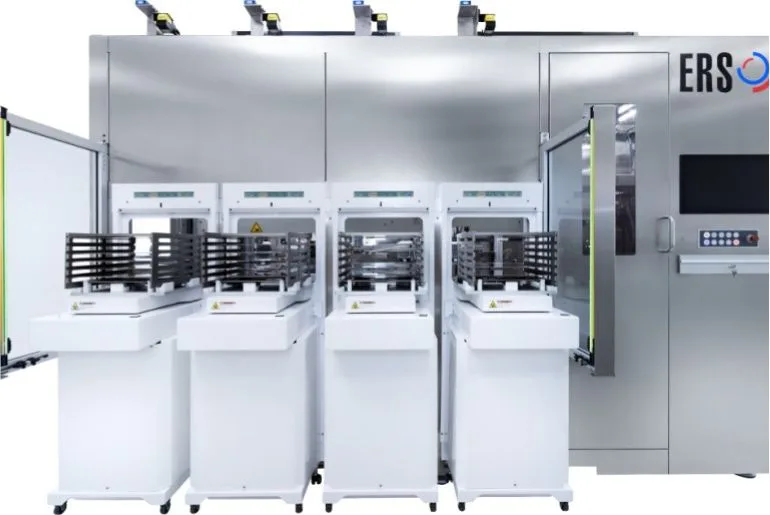
ERS electronic has introduced a fully automated panel-level packaging (PLP) tool engineered for 310×310mm rectangular substrates, delivering its first production unit to a tier-one semiconductor manufacturer for inline fab deployment. The platform consolidates three thermally critical backend steps—temporary carrier bonding, thermal debonding, and mechanical detaping—into an unbroken automation sequence capable of processing 13 panels per hour.
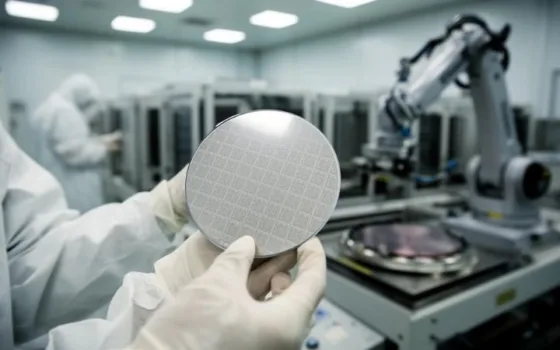
As artificial intelligence hardware and high-performance computing push conventional packaging to its physical limits, the industry is shifting beyond standard 300mm circular silicon wafers. Panel-level form factors provide substantially higher usable surface area, reducing edge-exclusion waste and improving silicon real estate economics for outsourced semiconductor assembly and test (OSAT) providers. According to market projections from Yole Group, the panel-level packaging sector is poised to expand at a compound annual growth rate exceeding 40% over the next five years. However, handling ultra-thin, large-area panel substrates without inducing mechanical warpage, die shift, or thermal stress remains an ongoing operational challenge.
This manufacturing hurdle becomes acute in dual-carrier processing workflows, which are essential for backside power delivery networks, through-silicon via (TSV) reveals, and backside metallization in 3D IC, 2.5D integration, and High Bandwidth Memory (HBM) architectures. Traditionally, carrier bonding, debonding, and tape removal have operated on standalone tools situated across different bays of an packaging facility. Shuttling thinned substrates between disparate equipment stations introduces latency, increases human and robotic handling risks, and exposes fragile dies to micro-cracking and particulate contamination.
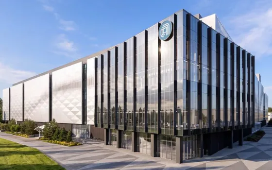
ERS electronic addresses these bottlenecks by consolidating the entire workflow within a modular, footprint-optimized machine architecture. Developed and built at the company’s Advanced Packaging facility in Barbing, Germany, the system leverages more than five decades of specialized thermal management and equipment design. By enabling panels to transition internally between dedicated processing chambers rather than traversing fab cleanroom floors, the tool preserves thermal continuity, maintains vacuum stability, and minimizes mechanical strain on fragile interconnects.
The delivery of this inline tool represents a notable milestone in transitioning panel-level packaging from pilot research to high-volume manufacturing. Laurent Giai-Miniet, CEO of ERS electronic, noted that unifying three traditionally fragmented process steps directly addresses customer demands for higher process consistency, yield improvements, and elevated throughput. As advanced packaging capacity remains a defining choke point in scaling next-generation AI processors and high-density chiplets, deploying integrated, high-throughput panel automation tools provides chipmakers with the manufacturing stability necessary to scale large-format advanced packaging lines profitably.