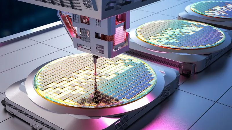
Atomera Incorporated has entered into a Joint Development Agreement with compound semiconductor wafer specialist IQE plc to develop and commercialize high-performance, cost-effective radio frequency Gallium Nitride (RF GaN) solutions. The strategic collaboration pairs Atomera’s proprietary Mears Silicon Technology (MST) on silicon base substrates with IQE’s high-volume compound semiconductor epitaxial growth capabilities. The project focuses initially on overcoming persistent cost and linearity barriers in high-volume RF markets, while establishing an engineering pathway toward commercial wafer supply for global foundries, integrated device manufacturers (IDMs), and fabless design houses.
Gallium Nitride has emerged as a cornerstone wide-bandgap material for high-frequency wireless communications, military radar, and telecommunications infrastructure due to its high electron mobility and power density. However, widespread commercial deployment across price-sensitive consumer and cellular RF front-end architectures has faced manufacturing bottlenecks. Conventional RF GaN devices have historically relied on silicon carbide (SiC) base substrates, which provide excellent thermal and lattice matching but incur substantial material costs and wafer diameter limitations. Growing GaN layers directly onto lower-cost silicon substrates resolves raw material expense, yet large lattice and thermal mismatches between silicon and GaN can cause substrate warpage, parasitic substrate conduction, and severe signal loss.
The joint program directly targets these physical limitations by applying MST to standard silicon wafers prior to compound layer growth. MST represents an atomically engineered, ultra-thin epitaxial silicon layer designed to improve transistor performance, suppress parasitic leakages, and optimize channel charge carrier flow. Under the bilateral framework, joint engineering teams from Atomera and IQE will execute a multi-cycle development sequence to co-optimize the underlying multi-layer transition stack. By refining epitaxial deposition over MST-treated silicon, the companies aim to demonstrate best-in-class RF linearity and minimal insertion loss across high-frequency bands.
The collaboration carries notable commercial implications for the semiconductor manufacturing supply chain. Rather than serving merely as a research partner, IQE provides the scalable manufacturing footprint required to transition the resulting MST-enabled GaN-on-silicon wafers into commercial production. The joint project will culminate in the fabrication and testing of qualified engineering samples, facilitating formal customer engagements across pure-play foundries and fabless RF chip architects.
Beyond cellular front-end modules and base station transceivers, the joint agreement provides flexibility for the partners to expand development into adjacent applications, including high-efficiency GaN power electronics. As mobile networks transition toward 5G-Advanced and early 6G baselines, RF architectures demand higher power efficiency in smaller physical footprints. By demonstrating high-volume epitaxial recipes on scalable silicon wafers, the Atomera-IQE partnership establishes a manufacturing foundation to transition RF GaN from premium niche sockets into mainstream communications hardware.