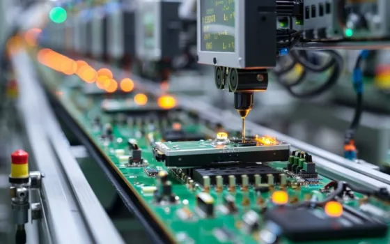
Samsung Electronics and SK Hynix are moving forward with major technology upgrades across their wafer fabrication plants in China, converting operational lines to produce advanced 3D NAND flash memory chips featuring more than 200 layers. The strategic tooling adjustments aim to meet escalating global storage demand fueled by artificial intelligence infrastructure while defending market share against domestic Chinese competitor Yangtze Memory Technologies Corp (YMTC). Both South Korean semiconductor manufacturers confirmed that upgrades are progressing in coordination with regulatory frameworks in Washington.
The operational pivots occur against a complex regulatory backdrop. Since the United States introduced multilateral export controls on advanced semiconductor equipment in 2022, foreign chipmakers operating fabrication lines in China have been required to secure annual licences to install US-origin tools, such as high-aspect-ratio plasma etching systems.Although the US Commerce Department’s Bureau of Industry and Security (BIS) stated in 2025 that it did not intend to grant authorisations for expanding net capacity or advancing baseline technology tiers at foreign-owned sites in China,both companies are retooling existing cleanroom footprints to align local production with yields achieved in South Korea.
At its primary manufacturing base in Xian—which accounts for approximately 40% of Samsung’s total global NAND wafer output—Samsung is executing an internal project designated as “Monami.” The facility currently produces roughly 200-layer flash memory. Samsung plans to convert the site to manufacture 286-layer V9 NAND dies, targeting an initial monthly run of 5,000 wafers by December 2026 before ramping to 40,000 wafers per month by December 2027. Samsung emphasized that these upgrades comply with US export rules, noting the project targets growing demand from international customers, including US data centre operators, without expanding overall physical wafer capacity or adding new structures.
Concurrently, SK Hynix is preparing to transition its Dalian site in north-eastern China to manufacture NAND architectures exceeding 240 layers, up from its existing 192-layer baseline. Acquired from Intel in 2021, the Dalian plant serves as the sole dedicated manufacturing hub for SK Hynix’s Solidigm subsidiary. Reports indicate SK Hynix holds authorization to produce up to 240 layers at Dalian and may pursue regulatory clearance for 300-plus-layer research and development to establish manufacturing baselines for prospective US facilities.
The push to upgrade follows significant market shifts within China’s memory landscape. According to market data from Omdia, YMTC captured 38.5% of the domestic Chinese NAND market in the second quarter of 2026, rising from 28% across 2025 and surpassing Samsung. During the same period, Samsung’s domestic market share receded to 33.5% while SK Hynix fell to 17%. With YMTC already fabricating 232-layer and select 294-layer chips, upgrading Xian and Dalian to higher layer densities is essential for the South Korean memory leaders to maintain commercial parity and secure the enterprise solid-state drive supply chains powering modern AI clusters.