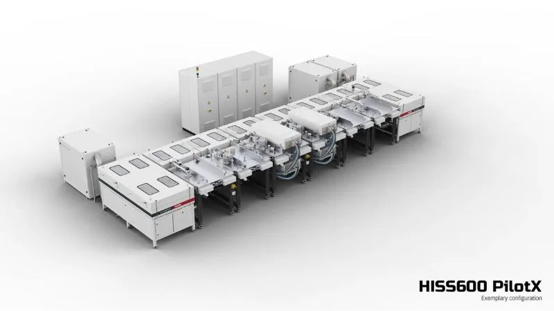
VON ARDENNE has expanded its semiconductor physical vapor deposition portfolio into panel-level packaging (PLP), deploying high-power impulse magnetron sputtering (HiPIMS) technology on its proprietary HISS modular horizontal coating platform. The manufacturing platform enables the industrial-scale deposition of high-aspect-ratio barrier and seed layers within through-glass via (TGV) structures and high-density redistribution layers (RDL). The development transitions advanced magnetron sputtering from standard circular wafer formats to large-area rectangular glass and organic panels, directly addressing manufacturing yield bottlenecks in high-density multi-die integration.
As artificial intelligence workloads and high-performance computing accelerators exceed the reticle limits of monolithic silicon, advanced packaging architectures increasingly depend on larger form factors and alternative substrate materials. Glass core substrates, in particular, offer superior dimensional stability, thermal endurance, and electrical performance over traditional organic cores. However, depositing conformal, defect-free metallic thin films into microscopic through-glass via holes with high aspect ratios presents acute processing hurdles. Conventional physical vapor deposition techniques often encounter poor sidewall step coverage, uneven film densities, and compromised interfacial adhesion, which can result in interconnect delamination and package failure under thermal stress.
The HiPIMS architecture addresses these physical limitations by generating high-density plasma discharge pulses, producing a higher ionization fraction of sputtered metal atoms than conventional direct-current sputtering. This allows the ionized coating flux to be directed into deep, narrow via holes, forming dense, highly adherent barrier and adhesion films. Dr. Holger Pröhl, Head of Technology and Application at VON ARDENNE, noted that enhanced adhesion and denser thin films reduce downstream rework, increase device operating life, and eliminate redundant processing steps, allowing semiconductor manufacturers to lift yields while expanding into high-performance product segments.
The transition to panel formats delivers substantial economic benefits over traditional 300mm wafer handling by dramatically increasing usable surface area and cutting-edge exclusion waste. According to data from Yole Group, the panel-level packaging sector generated more than $300 million in revenue in 2025 and is projected to expand at a compound annual growth rate exceeding 40% through 2030. Industry adoption is projected to accelerate sharply toward the end of the decade as leading foundries, including TSMC, establish commercial panel lines for AI and high-performance computing substrates.
Guido Ueberreiter, Vice President of Semiconductor Strategy at VON ARDENNE, emphasized that combining a scalable equipment architecture with advanced deposition physics enables manufacturers to transfer proven wafer recipes to panel substrates without compromising strict film uniformity standards. By qualifying industrial vacuum equipment capable of handling high-aspect-ratio metallization across large glass panels, equipment vendors are establishing the foundational toolsets required to transition next-generation heterogeneous integration into volume production.