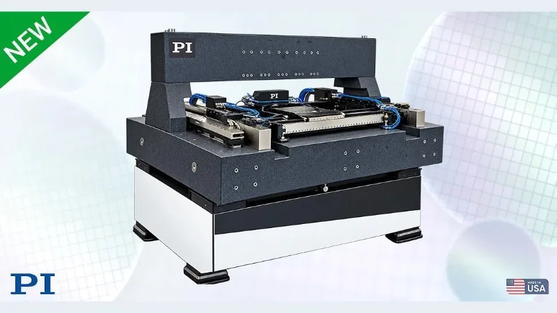
Physik Instrumente (PI) has unveiled the A-323 planar air bearing scanner at SEMICON West 2026, introducing a high-dynamic precision motion platform engineered for semiconductor inspection, optical metrology, photonics alignment, and laser micromachining. Designed and manufactured by PI engineers in the United States, the platform builds on the company’s earlier A-322 series, restructuring mechanical load transfer and axis architecture to achieve higher acceleration, shorter step-and-settle times, and sub-micron positioning repeatability.
In high-volume wafer fabrication, metrology and inspection throughput is constrained not only by velocity across the substrate, but by how rapidly optical or acoustic sensors can stabilize and capture measurements once motion halts. As advanced logic nodes, high-density 3D NAND, and heterogeneous chiplet packaging shrink defect tolerance margins, inline inspection tools must execute dense step-and-settle routines without introducing mechanical resonance into sensitive imaging optics. The A-323 addresses this bottleneck through an XY travel envelope of 500 × 500 mm, velocities reaching 2 m/s, acceleration up to 2 g, and an accuracy specification of 0.1 µm, with pitch and yaw constrained to 10 µrad and 2 µrad, respectively.
The mechanical redesign introduces three structural modifications to preserve dynamic stability. First, the scanner diverts motor reaction forces directly into the external machine chassis rather than the granite base. This isolates the granite assembly and its bridge-mounted optical lenses, cameras, and interferometric sensors from kinetic shocks, allowing optical data acquisition to begin earlier. Second, a split-beam cross-axis geometry places the payload close to the motor force plane. This configuration suppresses rocking during rapid accelerations and reduces the offset to the optical encoder plane, curtailing Abbe errors caused by angular deviations. Third, the platform widens the spacing between drive motors and optical encoders compared to the prior A-322 Ultra model. This expanded footprint improves control over vertical-axis yaw, preventing positioning drift at the critical outer edges of 300 mm wafers.
Equipment configurability remains central to cleanroom tool integration. The A-323 incorporates a central pocket designed to host application-tailored motion axes—such as PI’s A-523 Z-tip/tilt stage, a 5 mm vertical Z-stage, or combined rotary/tilt assemblies—while keeping the center of gravity low. The platform features newly engineered air-bearing pucks with higher film stiffness, integrated pneumatic routing, and symmetrical cable tracks that prevent position-dependent drag forces. Liquid-cooled motors mitigate thermal dissipation into the base frame, allowing capital equipment manufacturers to size drive units according to production duty cycles.
As wafer fabs expand capacity for advanced nodes and multi-die packaging, deploying motion stages that combine 2 g dynamics with frictionless air-bearing suspension provides tool builders with the mechanical stability needed to maximize wafer inspection units per hour.