Category: Packaging & Testing
October 18, 2026 · 2 mins read
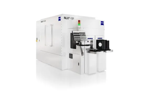
ZEISS Semiconductor Manufacturing Technology (SMT) has broadened its semiconductor equipment portfolio into advanced backend processing by introducing two metrology and process control platforms: ZEISS […]

October 16, 2026 · 2 mins read
The Government of Tamil Nadu has officially launched the Tamil Nadu Semiconductor Ecosystem Scheme 2026, establishing a targeted policy framework with state subsidies of […]

October 16, 2026 · 5 mins read
Two-dimensional (2D) semiconductors, only a few atomic layers thick, are a promising material for making AI chips faster and more energy efficient by stacking […]

October 16, 2026 · 2 mins read
Great Lakes Semiconductor (GLS) has unveiled the inaugural development under its Great American ChipForge™ platform, executed through the company’s Innovation Funnel™ initiative. The project […]

October 15, 2026 · 2 mins read
Eliyan has introduced its NuLight™ chiplet platform, presenting what it designates as the semiconductor industry’s first two-dimensional microVCSEL optical interconnect architecture. Unveiled at the […]
October 15, 2026 · 6 mins read
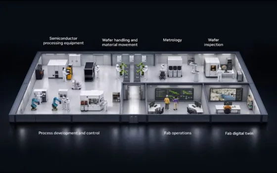
NVIDIA announced semiconductor leaders are adopting NVIDIA CUDA-X™ libraries — including the new NVIDIA cuPotential library, which developers can use to build AI agents […]

October 15, 2026 · 2 mins read
Great Lakes Semiconductor (GLS) has announced the inaugural project under its Great American ChipForge™ platform, launched via the company’s Innovation Funnel™ initiative. The development […]
October 14, 2026 · 2 mins read
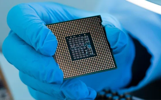
FUJIFILM Corporation has announced an $18 million (approximately ¥3 billion) investment to enhance and diversify chemical mechanical planarization (CMP) slurry production at its FUJIFILM […]

October 14, 2026 · 3 mins read
The International Semiconductor Industry Group (ISIG) will host the ISIG Executive Summit India 2026 at The LaLiT, New Delhi on 3-4 November 2026, bringing […]
October 13, 2026 · 2 mins read
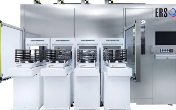
ERS electronic has introduced a fully automated panel-level packaging (PLP) tool engineered for 310×310mm rectangular substrates, delivering its first production unit to a tier-one […]
