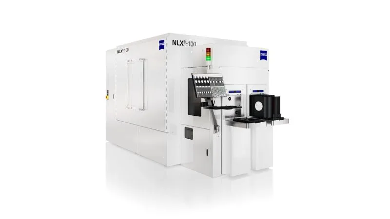
ZEISS Semiconductor Manufacturing Technology (SMT) has broadened its semiconductor equipment portfolio into advanced backend processing by introducing two metrology and process control platforms: ZEISS NLX and ZEISS DUNE. Showcased at SEMICON West, the tools target critical yield bottlenecks in multi-die packaging, specifically non-destructive volumetric inspection of hidden interconnects and dynamic wafer warpage correction across 300-millimeter substrates.
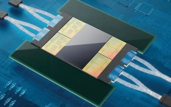
As artificial intelligence accelerators, high-performance computing silicon, and high-bandwidth memory (HBM) move toward heterogeneous integration, advanced packaging architectures are supplanting conventional monolithic scaling. Bringing multiple active chiplets together into compact 2.5D and 3D System-in-Package (SiP) structures creates microscopic vertical interconnects, through-silicon vias (TSVs), micro-bumps, and direct hybrid bonding interfaces. Because these connections are buried beneath multiple silicon layers, traditional optical and electron-beam metrology tools cannot evaluate physical integrity without destructive cross-sectioning.
The ZEISS NLX platform resolves this limitation by delivering non-destructive, high-resolution inline 3D X-ray inspection directly on 300mm production wafers. Engineered for pilot-line process qualification and high-volume manufacturing, the system allows packaging foundries and OSAT providers to inspect micro-bump alignment, solder wetting, voids, and bonding interfaces between stacked dies. Detecting latent structural defects before final encapsulation protects overall assembly yield and eliminates the scrap of expensive host dies.
Complementing volumetric defect inspection, ZEISS DUNE directly targets wafer bow and mechanical deformation. As wafers undergo iterative thermal cycles, thin-film deposition, chemical mechanical planarization, and multi-tier thinning, mismatched coefficients of thermal expansion across materials induce severe mechanical stress and wafer curvature. Excessive warpage prevents precise chucking, induces focal plane errors during lithographic overlay, and causes catastrophic bonding delamination during die-to-wafer or wafer-to-wafer hybrid bonding. ZEISS DUNE measures wafer topography at high spatial resolution and executes targeted corrections, stabilizing wafer shape to ensure smooth handoffs to downstream bonding and packaging tools.
The rollout marks a strategic expansion for ZEISS SMT beyond its foundational leadership in EUV lithography optics and photomask qualification platforms such as AIMS® EUV 3.0 and MeRiT defect repair systems. Christoph Hensche, President of ZEISS Semiconductor Manufacturing Optics, noted that advancing next-generation semiconductor manufacturing requires tight coordination across multiple complex manufacturing stages, combining optical expertise with advanced packaging process control. Axel Christian, President of ZEISS North America, highlighted the importance of close customer partnerships as ZEISS marks 100 years in the United States.
For the semiconductor industry, deploying high-throughput, non-destructive inline metrology and active warpage management provides the manufacturing repeatability required to scale 3D chiplet integration profitably. By addressing buried structural defects and wafer topography directly within the production flow, ZEISS provides essential toolsets to support commercial yield ramps across high-density AI hardware.