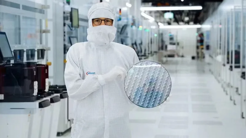
Infineon Technologies AG is establishing the world’s first high-volume manufacturing facility for next-generation gallium nitride (GaN) power semiconductors on 300-millimetre wafers at its Villach site in Austria. The semiconductor supplier plans to invest approximately €1.1 billion through 2034 by upgrading and leveraging its existing cleanroom facilities, with commercial volume production scheduled to begin by the end of 2027.
The project represents a crucial industrial transition for wide-bandgap semiconductors from legacy 200mm wafer substrates to 300mm diameter processing. Chip production on 300mm wafers yields roughly 2.3 times as many dies per wafer compared to 200mm lines, providing Infineon with major manufacturing efficiencies and economies of scale. Having successfully processed initial 300mm GaN wafers two years ago, Infineon is now transferring the technology into commercial high-volume lines to serve expanding applications across artificial intelligence data centres, energy infrastructure, electric mobility, industrial robotics, and consumer electronics.
The facility expansion is supported under the framework of the European Chips Act, with the European Commission formally approving up to €319 million in state aid from the Austrian Federal Ministry for Economic Affairs, Energy and Tourism. Jochen Hanebeck, Chief Executive Officer of Infineon Technologies AG, noted that the investment underlines the company’s commitment to strengthening the European semiconductor ecosystem and technological sovereignty by becoming the first globally to bring 300mm GaN power electronics to mass production. Austrian Federal Chancellor Christian Stocker stated that the billion-euro project represents one of the largest single investments in Austria’s high-tech manufacturing sector, bolstering European industrial competitiveness. Austrian Federal Minister for Economic Affairs Wolfgang Hattmannsdorfer highlighted that the public funding will anchor high-value manufacturing and semiconductor research within the continent, noting that every direct job in chip manufacturing supports six jobs across the wider economy.
For the international semiconductor industry, moving GaN to 300mm lines is essential to meet surging efficiency demands. Hyperscale AI data centres require power supply architectures with superior power density and minimal thermal dissipation, characteristics where GaN surpasses conventional silicon switches. Market analysts project the global market for GaN power semiconductors to grow from 2025 to approximately USD 3.5 billion by 2031, representing a compound annual growth rate of around 35 percent.
Sabine Herlitschka, Chief Executive Officer of Infineon Technologies Austria AG, emphasized that the Villach expansion translates domestic microelectronics research into industrial value creation while strengthening Europe’s strategic autonomy. Villach anchors a dedicated workforce of 4,800 employees and acts as a global competence centre for power electronics and new semiconductor materials. By combining scaled 300mm wafer manufacturing with front-end wide-bandgap research, Infineon is establishing an integrated manufacturing base capable of delivering cost-effective, high-efficiency GaN power semiconductors to the global market.