Great Lakes Semiconductor (GLS) has unveiled the inaugural development under its Great American ChipForge™ platform, executed through the company’s Innovation Funnel™ initiative. The project leverages GLS design centers, proprietary ChipForge modular wafer fabrication lines, and its FINPAT™ packaging and test architecture to deliver intelligent, AI-enabled multi-sensor solutions for commercial vehicle platforms. The milestone demonstrates a distributed, end-to-end manufacturing model designed to accelerate prototype turnaround and lower traditional barriers to specialized silicon production.
The initiative unites an international ecosystem covering design, tool manufacturing, materials, and packaging. GLS is collaborating with Japanese equipment specialists Neitas and Daikin on modular fabrication hardware, while Altascient provides predictive-intelligence planning tools. On the component side, FMC supplies low-power ferroelectric semiconductor memory, while BlueDot Ventures provides low-energy sensors derived from platforms already operating across commercial vehicle fleets. Advanced Printed Electronic Solutions (APES) joins through the FINPAT framework, developing an additively manufactured package substrate that enables the direct heterogeneous packaging of GLS and FMC silicon alongside BlueDot sensors.
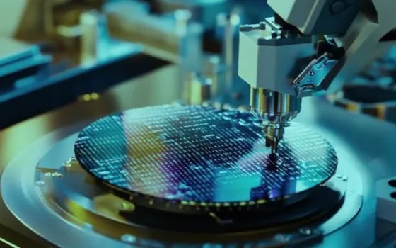
At the core of the deployment is the ChipForge fabrication concept, developed as an agile alternative to high-overhead conventional mega-fabs. Built around configurable production lines, the platform supports multiple process technologies, device architectures, and substrate materials without requiring the wholesale rebuilding of cleanroom bays. Dr. Richard Thurston, Chairman and Chief Executive Officer of GLS, highlighted that aligning manufacturing process blueprints from initial design concepts through production scale enables engineering teams to turn concepts rapidly into qualified, packaged prototypes. Validated process flows within ChipForge are structured to transfer smoothly to high-volume foundry partners as commercial demand scales.
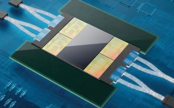
The technical execution underscores how heterogeneous integration resolves edge computing constraints in vehicle electronics. At the APES Fishkill facility in New York, engineers are utilizing additive manufacturing techniques to embed energy-harvesting structures, supercapacitors, and printed electronics directly into reusable power module substrates. By co-packaging FMC ferroelectric memory chiplets with a GLS-optimized RISC-V core running an energy-efficient machine learning classifier, the multi-chip module processes edge inference locally. Because the ferroelectric memory retains learned model parameters with negligible power draw while the processor sleeps, the platform cuts duty-cycle energy consumption.
The project highlights a transition toward distributed semiconductor manufacturing and agile packaging workflows. By combining modular front-end wafer fabrication with additive advanced packaging, GLS and its partners provide a capital-efficient pathway to transition custom automotive silicon from research environments into qualified commercial hardware.