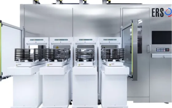
As traditional silicon scaling slows, advanced packaging has become the semiconductor sector’s most critical lever for delivering faster, smaller, and more power-efficient devices. To bridge the gap between pilot-line innovation and mass manufacturing, the Global Electronics Association has signed a Memorandum of Understanding (MoU) with the Fraunhofer Group for Microelectronics.
The alliance centers on the APECS pilot line, Europe’s initiative for advanced packaging and heterogeneous integration established under the EU Chips Act. Coordinated by the Fraunhofer-Gesellschaft and operated through the Research Fab Microelectronics Germany (FMD)—an alliance linking 13 Fraunhofer institutes and two Leibniz institutes—APECS offers cutting-edge infrastructure for 2.5D/3D integration and modular chiplet architectures.
While pilot lines excel at proving out complex architectures, turning novel lab designs into commercially viable silicon remains difficult. Without unified standards across design rules, material selection, testing, and reliability, scaling up creates costly production bottlenecks.
This partnership combines APECS’s physical fabrication capabilities with the Global Electronics Association’s global footprint in standards development and supply chain alignment. The initiative places heavy focus on System-Technology Co-Optimization (STCO), an engineering approach that synchronizes chip design, packaging materials, and assembly workflows early in product development. These standardized methods ensure modern packaging can reliably integrate heterogeneous dies, including high-frequency RF modules and AI accelerators, into unified systems.
“Our silicon to systems approach maps to the reality that advanced packaging changes the rules for everyone, not just one segment of the supply chain,” said Matt Kelly, chief technology officer at the Global Electronics Association. “Collaborations like this are about building the practical scaffolding—guidelines, standards, tools, and training—that helps suppliers qualify, customers specify, factories operate, and regulators trust.”
Following an official project launch on September 24, both organizations will prioritize creating standardized test guidelines, design data interfaces, and qualification frameworks.
“For these capabilities to translate into industrial use, technical development needs to reflect standards and common interfaces early,” said Dr. Dirk Schumann, director of the APECS pilot line. By grounding R&D in real-world factory requirements, the partnership will de-risk high-volume manufacturing and bolster Europe’s semiconductor supply chain resilience.