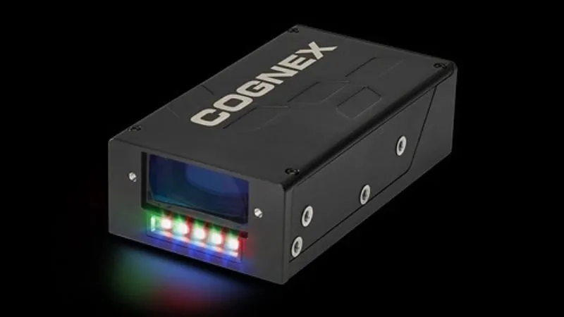
As global semiconductor fabrication facilities accelerate capital expenditures to meet surging demand for high-performance computing, cleanroom operations face an intensifying operational challenge: microscopic-level lot tracking across non-standard substrates. Cognex Corporation has introduced the In-Sight® 1750 Series, an automated wafer and panel identification reader engineered specifically to eliminate yield-sapping read failures across front-end fab and back-end packaging lines.
In contemporary silicon processing, every individual wafer undergoes hundreds of chemical, thermal, and mechanical cycles—from extreme ultraviolet (EUV) photolithography and reactive ion etching to chemical mechanical planarization (CMP). Throughout these stages, alphanumeric codes and 2D matrix symbols scribed onto wafer bevels or notch regions suffer severe optical degradation. Low mark-to-background contrast, film deposition over laser marks, oxide layer variations, and rough backing surfaces routinely defeat traditional optical character recognition (OCR) systems.
When a wafer reader at an automated transport carrier or process tool fails, equipment stops. An operator must enter the cleanroom environment or manually intervene via terminal override. This manual troubleshooting breaks Overall Equipment Effectiveness (OEE) metrics, introduces particulate contamination risks, and clouds statistical process control (SPC) data.
The In-Sight 1750 addresses these physical-layer inspection hurdles through a re-engineered optical pipeline. The system combines narrow-band, purpose-built multi-angle illumination with high-dynamic-range imaging to cut through glare, surface roughness, and semi-transparent thin films. These optical subsystems work in tandem with embedded algorithmic decoding, which leverages targeted AI edge models to decipher heavily degraded, low-contrast, and deformed dot-matrix markings without requiring continuous manual retraining. By confining machine learning strictly to localized edge-pattern reconstruction, the reader ensures rapid, deterministic cycle times suitable for high-speed wafer-handling robotics.
Beyond silicon, modern advanced packaging architectures—such as 2.5D/3D chiplet stacking and high-density fan-out wafer-level packaging (FOWLP)—rely on large panel substrates, reconstructed molded wafers, and glass carriers. These materials display significant warpage, high reflectivity, and varied chemical resistance properties that confound standard vision sensors. The In-Sight 1750 is built to handle both wafer notches and panel edges across these specialized materials, maintaining consistent identification across heterogeneous packaging workflows.
To reduce tool integration overhead, Cognex designed the hardware footprint and operational logic as an in-place upgrade path for the widely deployed In-Sight 1740 platform. Tool manufacturers (OEMs) and fab automation engineers can import legacy recipes and job configurations directly, bypassing protracted mechanical retrofits or SECS/GEM communication interface redesigns.
A newly integrated web-based configuration utility enables remote recipe tuning from outside the cleanroom gowning boundary, while automated read-audit logging provides end-to-end traceability records required by automotive and mission-critical device standards. By addressing raw physical-layer visibility at the tool interface, the system helps modern fabs sustain operational cadence across increasingly complex multi-die manufacturing nodes.