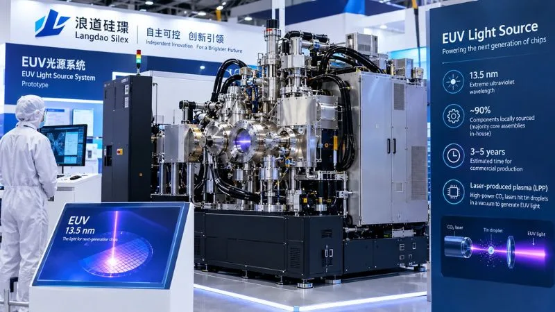
Shanghai-based semiconductor equipment startup Langdao Silex has publicly displayed a prototype extreme ultraviolet (EUV) light-source system at the China International Industry Fair in Shanghai. The emergence of an operational light source—the central subsystem responsible for generating 13.5-nanometer radiation to print nanoscale transistor features onto silicon wafers—represents a notable milestone in China’s ongoing drive to develop sovereign wafer-fabrication toolchains.
The company stated that approximately 90 percent of the prototype system’s components are domestically sourced, with the majority of the core assemblies developed directly in-house. While the system marks a transition from academic research to hardware prototyping, on-site technical personnel indicated that commercial volume production remains an estimated three to five years away. Developing laser-produced plasma (LPP) EUV sources involves complex technical requirements, including pulsing high-power CO2 lasers against microscopic molten tin droplets tens of thousands of times per second in a high-vacuum chamber to produce extreme ultraviolet light at sufficient power and stability for high-volume wafer fabrication.
Founded in 2024, Langdao Silex originated from research conducted within Tsinghua University’s Gas Discharge and Plasma Laboratory, which specializes in laser-produced plasma mechanisms. The venture has attracted investment from state-backed vehicles and strategic semiconductor funds, including China Fortune-Tech Capital, an investment arm affiliated with Semiconductor Manufacturing International Corporation (SMIC). China’s advanced foundries remain restricted from purchasing commercial EUV lithography platforms from Dutch manufacturer ASML under multilateral export controls. Consequently, domestic fabs have relied on deep ultraviolet (DUV) immersion scanners and complex multi-patterning schemes to fabricate advanced logic, which increases mask counts, reduces wafer throughput, and impacts production yields.
The light source is one part of a larger push by Chinese toolmakers across the wafer fab equipment sector. At concurrent domestic industrial exhibitions, local equipment vendors showcased medium-current ion implanters and advanced thin-film deposition tools. Industry projections from Bernstein Research indicate domestic tool suppliers are positioned to capture 52 percent of China’s wafer-fabrication equipment market by 2028, expanding from an estimated 28 percent this year.
However, translating a prototype light source into a production-grade lithography scanner presents extensive engineering challenges. Beyond generating stable EUV power, an operational scanner requires ultra-precise reflective projection optics, high-acceleration vacuum wafer stages, and specialized photoresists. While the prototype demonstrates progress in domestic plasma source physics, integrating these elements into a commercial tool capable of matching global fab productivity standards remains a multi-year development effort.