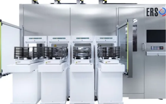
For nearly sixty years, Singapore has steadily built itself into a cornerstone of the global electronics map. Today, the island nation produces one in ten chips worldwide and builds one-fifth of all global semiconductor manufacturing equipment. Now, the country is taking a decisive step to bring its entire microelectronics ecosystem under a single national identity: SG Semiconductor.
Announced by Dr. Tan See Leng, Minister for Trade and Industry (Energy and Industry), at the Innovate Together 2026 forum, SG Semiconductor is jointly spearheaded by the Agency for Science, Technology and Research (A*STAR) and the Singapore Economic Development Board (EDB). Rather than operating as isolated labs and individual factories, the initiative unites public research, universities, global equipment makers, foundries, and local talent under one unified banner.
A $800 Million Push Across 7 Key Pillars
Backed by a fresh S$800 million commitment from 2026 to 2030 under the RIE Flagship in Semiconductors, the new identity focuses heavily on bridging public sector research with commercial manufacturing.
SG Semiconductor has mapped out seven strategic hardware disciplines designed to address high-demand markets like artificial intelligence hardware, high-speed data communications, and industrial sensing:
-
Advanced Packaging: Pushing chiplet-style heterogeneous integration to beat classic transistor limits.
-
Silicon Photonics: Speeding optical interconnects for next-gen data centers and supercomputers.
-
Power Electronics: Enhancing power efficiency for electrified mobility and industrial systems.
-
RF GaN (Gallium Nitride): Boosting high-frequency communications and defense hardware.
-
PiezoMEMS: Advancing precision micro-sensors for intelligent systems.
-
Flat Optics: Miniaturizing advanced optical systems.
-
IC Design: Driving new architectural breakthroughs from local design teams.
Global Tech Giants Deepen Local Roots
To prove SG Semiconductor is more than just a branding exercise, several high-impact industry alliances were unveiled at the forum:
-
Advanced Packaging Expansion: Applied Materials and ASTAR launched Phase 4 of their joint laboratory, scaling up cleanroom equipment and engineering headcount to develop high-density architectures for AI compute. Concurrently, KLA joined hands with ASTAR to create a process control framework focused on boosting fab yield, while STATS ChipPAC teamed up with the agency to develop co-packaged optics (CPO) solutions for volume production.
-
Silicon Photonics on 300mm Wafers: GlobalFoundries deepened its R&D partnership with A*STAR to translate silicon photonics onto 300mm manufacturing lines in Singapore, giving high-performance data hardware a direct path from lab bench to volume fab.
-
Intelligent Robotics & Upstream Materials: Tacta Systems established Singapore operations and tapped A*STAR’s “Lab-in-Fab” platform for piezoMEMS prototyping. Upstream, the National Centre for Advanced Integrated Photonics (NCAIP) at NTU partnered with Battery Age Minerals to turn raw germanium into high-speed optical devices.
As global chip supply chains face geopolitical friction and rising design complexity, Singapore’s SG Semiconductor positions the country not just as a reliable manufacturing floor, but as a trusted, collaborative hub where next-generation chips are designed, proven, and built for world markets.