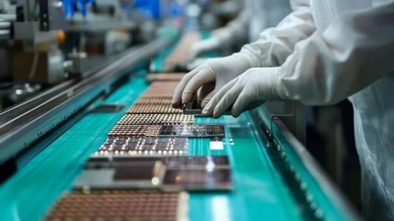
The Taiwan Semiconductor Manufacturing Company has recently unveiled huge expansion plans for their operations in Japan. This represents a big leap for the world of technology and semiconductors. According to the news coming from the company itself, it was revealed that the tech giant will produce advanced semiconductors through the use of 3-nanometre process technology in the second factory belonging to its Japan-based subsidiary, which is named as Japan Advanced Semiconductor Manufacturing.
The scale of financial investment required for the plan is huge; it is estimated that total investments in equipment alone would exceed the mark of 23 billion US dollars. The company officials made it clear that there won’t be any rush when it comes to implementation of the plan; instead, both investment and production would be done gradually in different phases. The gradual phase-wise implementation of the plan would allow them to keep pace with the ever-changing demands of the market. Moreover, the company made it clear that continuation of such plans would depend a lot upon government support.
This strategy will largely help to solve the problem of rising demand in the world for high-performing chips used for artificial intelligence projects. In today’s world of growing technology oriented towards artificial intelligence, smart computing and processing huge amount of data, the demand for compact, fast and efficient chips is skyrocketing. With the introduction of 3 nanometre technology in Japan, the plant will be able to provide these components not only to its customers in Japan, but also to many other countries around the world.
The subsidiary working on this project has been created through cooperation of the tech company with its industrial partners and represents a joint venture. The plants are located in Kumamoto, Japan, and can be considered to be an excellent addition to the capabilities of Japanese local production. In the past, creation of the advanced plants needed to concentrate the most advanced technology in home territories. However, current changes in the global market and geopolitics made the industry leaders look for diversification of production locations in friendly regions. Bringing 3 nanometre technology to Japan is an important step, as it brings the most advanced chip production technology out of Taiwan.
Beyond the construction of this particular factory, the scope of this partnership model is further expanding within the region. Prior to that, there had been partnership ventures between large names from industry such as Sony Semiconductor Solutions to create joint ventures to be located in another prefecture of Japan. Their focus was going to involve manufacturing of next-generation image sensors with a plan to commence commercial operations within this decade.
Generally, the examples provided reflect a wider change taking place in the global semiconductor industry. In times when many countries are working to assure their own stable sources of supply of vital electronic components, the magnitude of such investments shows importance of public-private collaboration and international partnerships. While expanding the capabilities in Japan, the scope of this process creates further support for the entire supply chain, making possible further development of technologies such as artificial intelligence and computing.