India’s move into semiconductor manufacturing represents one of the country’s most significant industrial pivots. Yet the conversation remains dominated by investment amounts, production targets, and technology roadmaps. A critical gap exists: the electrical infrastructure and power quality engineering that will determine the difference between competitive, reliable fabrication plants and facilities that struggle with yield loss, operational disruption, and cost overruns. This article examines why power infrastructure quality and resilience warrant equal prominence in India’s semiconductor strategy, and what engineering and policy approaches can ensure success.
The Semiconductor Infrastructure Reality
Modern semiconductor fabrication plants operate at a scale and precision that few industries match worldwide. A single advanced fab may consume up to 150 megawatts of continuous power — equivalent to supplying electricity to a mid-sized city of 100,000 homes. However, capacity is not the issue. The real challenge is a demanding problem of power stability, consistency, and purity at a level that conventional industrial infrastructure often cannot reliably provide.
Semiconductor manufacturing encompasses multiple precision stages: photolithography, ion implantation, chemical vapor deposition, etching, wafer inspection, and chiplet assembly. Each process relies on sophisticated equipment whose precision has advanced to the nanometer scale. The equipment contains hundreds of sensors, high-frequency power supplies, and precision motion controllers. Any instability in the incoming electrical power cascades through this entire chain, affecting final product quality and yield rates significantly.
India’s semiconductor policy framework recognizes the importance of dedicated fabs and technology nodes. However, infrastructure discussions frequently focus on visible physical assets: cleanrooms, water purification systems, specialty gas logistics, and human capital. Power quality and resilience engineering, despite being equally critical, remains under-emphasized in strategic conversations. This gap creates substantial risk for investors and policymakers.
Power Quality Events and Industry Impact
Voltage Sag Events and SEMI F47 Standards – The semiconductor industry has developed rigorous standards to quantify power quality requirements. The SEMI F47 specification defines minimum voltage sag immunity that all semiconductor processing equipment must achieve. The standard requires equipment to operate without interruption during voltage sags to 50 percent of nominal voltage lasting up to 200 milliseconds, sags to 70 percent for up to 500 milliseconds, and sags to 80 percent for up to one second.
The semiconductor industry has developed. the SEMI F47 specification to define minimum voltage sag immunity that all semiconductor processing equipment must achieve. The fundamental gap between India’s current grid reliability and the operating environment fabs require by way of SEMI F47 compliance is exposed. A single unplanned shutdown that may occur due to a voltage sag lasting milliseconds can cost millions of dollars: direct wafer loss, precision tool recalibration, cleanroom re-qualification, and extended recovery time. A single unplanned shutdown costs millions of dollars: direct wafer loss, precision tool recalibration, cleanroom re-qualification, and extended recovery time.
Harmonic distortion and voltage imbalance add further complexity. Modern grids with high penetration of switching power supplies, variable frequency drives, and renewable energy sources generate harmonic distortion reaching 5 to 10 percent or higher on heavily loaded networks. For semiconductor tools with tight frequency and phase angle tolerances, this distortion degrades process repeatability and introduces subtle defects appearing only in downstream testing.
The Indian Grid Context—India’s grid has expanded rapidly in total capacity. However, India’s System Average Interruption Frequency Index (SAIFI) stands at 2.39 outages per customer annually. and India’s System Average Interruption Duration Index (SAIDI) is approximately 3.72 hours annually.
In designated semiconductor hubs like Dholera, Gujarat, and YEIDA in Uttar Pradesh, much of the projected power supply links to solar parks and renewable energy sources. While renewable integration is essential for sustainability, renewables alone cannot provide the 24/7 baseload power fabs demand. Without sufficient coal, nuclear, or other stable generation backing the system, facilities face power variability that translates directly to production volatility.
Technical Architecture for Power Resilience
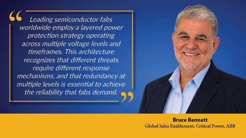
Layered Protection Strategy – Leading semiconductor fabs worldwide employ a layered power protection strategy operating across multiple voltage levels and timeframes. This architecture recognizes that different threats require different response mechanisms, and that redundancy at multiple levels is essential to achieve the reliability that fabs demand.
At the primary level, medium-voltage UPS systems provide protection against grid events lasting seconds to several minutes. These systems integrate with on-site generation and feature sub-cycle response time — detecting and responding to disturbances within microseconds, before equipment controllers register the event. At the secondary level, active voltage conditioners deployed at critical process tools provide continuous voltage regulation and instantaneous correction of sags and surges without requiring energy storage. At the tertiary level, low-voltage UPS systems protect control systems, automation networks, and IT infrastructure, ensuring the management layer remains operational during power events.
Each layer operates independently within its own timeframe and addresses distinct failure modes. Medium-voltage protection addresses grid-scale events. Equipment-level protection manages imbalances and local disturbances. Control-level protection ensures facility recoverability. This multi-layer approach is not simple redundancy — it is purpose-engineered resilience.
Integration with Secondary Power Sources -Most semiconductor fabs operate with either secondary transmission feeds or on-site generation: diesel generators, gas turbines, or increasingly, hybrid systems integrating renewables with battery storage. Power protection UPS systems must integrate seamlessly with this infrastructure. When grid conditions degrade, the UPS must support transition to secondary power without electrical disturbances affecting process equipment. This integration requires careful electrical design, synchronization protocols, and rigorous system testing during commissioning.
Modern UPS systems increasingly support grid ancillary services markets, where UPS owners receive compensation for providing grid support during stress periods. This creates secondary revenue streams that improve investment returns. Forward-looking fab operators are already evaluating these capabilities as part of their financial planning.
Total Cost of Ownership and Energy Efficiency
Semiconductor fab economics are driven by manufacturing yield, cost per unit, and long-term operating cost. Power protection systems represent significant capital investment and contribute materially to annual operating costs. A poorly specified UPS system can consume 8 to 10 percent of facility power in losses, representing millions of dollars annually over a 15 to 20-year lifespan.
Advanced static medium-voltage UPS technologies with ZISC architecture achieve more than 98 percent efficiency, compared with conventional systems at 92 to 94 percent. Over 15 years, this 4 to 6 percent improvement translates to 4 to 6 gigawatt-hours of energy saved, with corresponding reductions in operating cost and carbon footprint.
Active voltage conditioners, requiring no energy storage, achieve even higher efficiency because they operate without battery charge-discharge cycles. These systems cost-effectively protect against voltage sags while minimizing footprint and maintenance requirements. Facility planners should benchmark total cost of ownership across facility life, not simply first cost — this discipline consistently demonstrates that high-efficiency systems deliver superior long-term economics.
Policy and Infrastructure Planning Implications
Utility and Transmission Modernization – India’s semiconductor ambitions depend on power infrastructure that goes beyond capacity. Utilities and transmission operators must prioritize grid modernization in semiconductor zones: real-time monitoring capability, high-speed fault detection and isolation, redundant transmission feeds, and dynamic voltage support systems. Investment in grid infrastructure in zones like Dholera and YEIDA must match or exceed investment in fab construction itself.
Facility Design and Specification – Power protection for semiconductor fabs must be specified by electrical engineers with direct fab experience, working closely with equipment suppliers to understand facility and tool-level power quality requirements. This expertise must be engaged early in facility design, not after production planning begins. The difference between proactive electrical design and reactive retrofitting is often hundreds of millions of rupees in cost and months of schedule delay.
Standards Compliance and Benchmarking – All facility specifications must commit to SEMI F47 voltage sag immunity standards and IEC 61000 power quality standards. Compliance is not optional; it is foundational to reliable semiconductor manufacturing. Benchmarking against global fab standards ensures that new Indian facilities are competitive in reliability and operational efficiency, and can attract and retain high-value supply chain relationships.
The ABB Approach to Semiconductor Power Protection
ABB’s Critical Power business brings decades of experience deploying power protection solutions across semiconductor fabs worldwide, protecting hundreds of billions of dollars in production equipment and enabling trillions of dollars in semiconductor output. ABB is the only vendor with a comprehensive portfolio addressing power protection across all voltage levels and timeframes required in semiconductor facilities.
HiPerGuard, ABB’s medium-voltage UPS, operates at voltages up to 34.5 kilovolts and delivers 98 percent efficiency through its patented Impedance Isolated Static Converter (ZISC) architecture. It provides IEC 62040.3 Class 1 load protection with sub-cycle response, reacting to grid disturbances faster than the disturbance duration itself. Scalable from 2.5 megawatts to 25 megawatts in parallel configurations, it allows fabs to match investment to capacity growth. Maintenance intervals extend to ten years, reducing service disruptions. Real-time monitoring via ABB Ability enables predictive maintenance strategies.
The PCS100 AVC-40 Active Voltage Conditioner provides instantaneous correction of voltage sags and swells directly at process equipment level. Continuous regulation against undervoltage, overvoltage, and voltage imbalance protects expensive process tools from cumulative electrical stress and improves yield consistency. Operational efficiency exceeds 98 percent by drawing supplementary energy directly from the utility during sag events rather than relying on stored energy, eliminating battery maintenance overhead and floor-space constraints.
ABB’s low-voltage UPS portfolio — including Megaflex, PowerValue, DPA UPScale, and PowerWave families — completes the protection layer for control systems, automation networks, and facility IT infrastructure. This comprehensive portfolio enables facility designers to specify a complete power resilience architecture from medium-voltage intake through equipment-level protection to control system safeguarding.
India’s semiconductor ambitions needs equal emphasis on electrical infrastructure quality and resilience. Three strategic priorities emerge clearly from this analysis:
Integrate power protection specialists into facility planning from the earliest stages. Power infrastructure is not an afterthought; it is a production-critical input that shapes facility design, operating cost, and long-term competitiveness. Incorporating power resilience into design costs a fraction of the cost of retrofitting protection after commissioning.
Commit to technology and service partnerships with proven semiconductor credentials and in-country support. India’s fab buildout is a multi-decade undertaking. The infrastructure partners and technology choices made today will determine whether facilities deliver world-class, competitive results. Global semiconductor experience combined with local service presence are equally important.
Prioritize grid modernization investments in designated semiconductor zones. Generation, transmission, and distribution operators must be equal partners in India’s semiconductor strategy. Modern, resilient electrical infrastructure is an essential competitive advantage.
India possesses the policy framework, the financial commitment, and the manufacturing scale to become a genuine global semiconductor hub. Ensuring that electrical infrastructure foundations are correctly specified and appropriate power protection designs are deployed from day one will determine whether that ambition delivers competitive, reliable results.