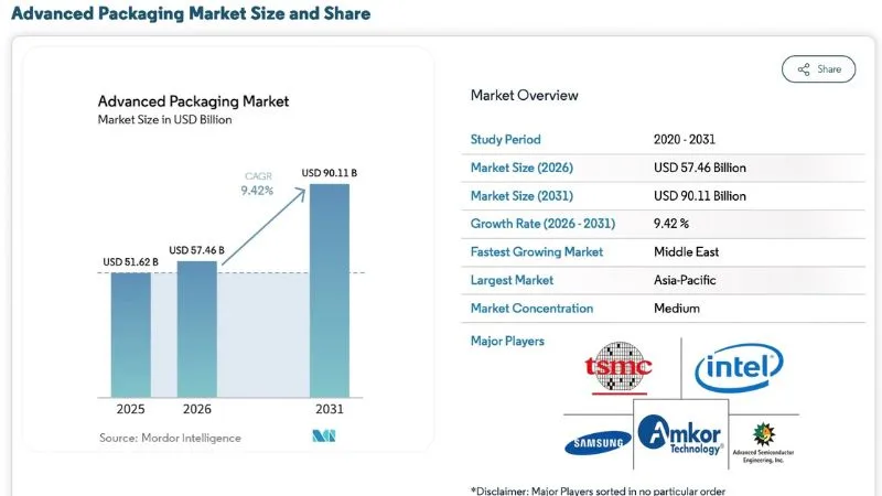
The advanced packaging market size is expected to grow from USD 51.62 billion in 2025 to USD 57.46 billion in 2026 and is forecast to reach USD 90.11 billion by 2031 at 9.42% CAGR over 2026-2031. Momentum is shifting from node-shrink economics to heterogeneous integration, where chiplets, interposers and stacked-die assemblies deliver power-efficient performance that conventional monolithic scaling can no longer support economically. Fan-out wafer-level and 2.5D interposer techniques are gaining importance as sovereign-AI mandates and export-control regimes encourage on-device inference architectures that minimize cross-border technology exposure. Automotive electrification is another structural driver, because silicon-carbide power modules need copper-pillar or hybrid-bond connections to survive thermal cycling far beyond the limits of legacy wire-bond assemblies. Finally, government subsidy programs across the United States, European Union and South Korea are localizing capacity and accelerating equipment purchases that otherwise would have faced multi-year payback hurdles.
Rising Demand for Heterogeneous Integration for AI and HPC
Chiplet architectures now partition logic, memory and I/O across multiple tiles connected by high-bandwidth interposers, enabling compute density that monolithic designs cannot reach within power limits. TSMC shipped more than 15 000 CoWoS wafers in 2025 for NVIDIA’s Hopper and Blackwell GPUs, highlighting commercial readiness. Intel’s Foveros Direct hybrid-bond technology achieves sub-10-micron pitch, cutting cache-to-core latency below 5 ns.[2] Mix-and-match logic, analog and RF tiles fabricated on different nodes optimize cost and time-to-market. The trend sustains double-digit expansion in 2.5D and 3D platforms that underpin data-center accelerators and sovereign-AI initiatives.
Miniaturization of Consumer Devices Boosting WLP Adoption
Smartphones and wearables target sub-6 mm Z-heights, leaving no room for substrate-based packages. Fan-out wafer-level technology redistributes I/O across the die surface, achieving package thickness below 0.4 mm. Apple and Qualcomm have already migrated high-volume processors to fan-out, and mid-tier Android brands follow as tooling costs amortize. Wearable biosensors are adopting fan-in chip-scale packages that eliminate wire bonds, enhancing shock resistance and hermeticity. As brands prioritize thinness and battery life, the advanced packaging market gains incremental wafer-level volume across consumer segments.
Government Semiconductor Subsidies (CHIPS and EU Chips Acts)
The United States CHIPS and Science Act dedicates USD 39 billion in direct grants plus USD 75 billion in loan guarantees, explicitly naming advanced packaging as a strategic capability. TSMC’s Arizona site, backed by USD 6.6 billion in grants, will start CoWoS production in 2025. The EU Chips Act channels EUR 43 billion (USD 49.6 billion) into regional pilot lines such as Fraunhofer’s panel-level facility in Dresden. South Korea’s KRW 26 trillion (USD 0.019 trillion) package expands Samsung’s Pyeongtaek capacity by 40%. Subsidy competition is redrawing supply chains and fragmenting the industry into regional clusters.
EV Power-Electronics Reliability Needs
Silicon-carbide MOSFET inverters face thermal cycles above 200 °C, forcing a move from wire bonds to copper-pillar and hybrid-bond connections that survive 15-year vehicle lifetimes. Infineon’s CoolSiC modules recorded zero field failures across 500 000 vehicles in 2024, validating advanced packaging for automotive power stages.[3] Tesla’s hybrid-bonded SiC modules cut parasitic inductance 30% and achieved 98.5% inverter efficiency. Automated optical inspection and X-ray laminography raise capex yet shrink warranty reserves, making reliability-centric packaging a core differentiator as battery costs decline.
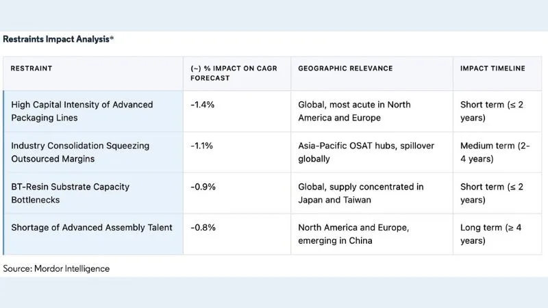
High Capital Intensity of Advanced Packaging Lines
Panel-level factories demand more than USD 500 million per line for lithography, electroplating and test equipment, stretching payback beyond five years at today’s utilizations. Hybrid-bonding tools priced above USD 15 million process only 30 wafers per hour, creating throughput pinch points. Depreciation cycles compress to three years because generations turn quickly, pushing operating margins for many OSATs below 15%. Government subsidies cover only 30–40% of project cost in high-wage regions, forcing private investors to bridge large funding gaps and delaying greenfield expansion.
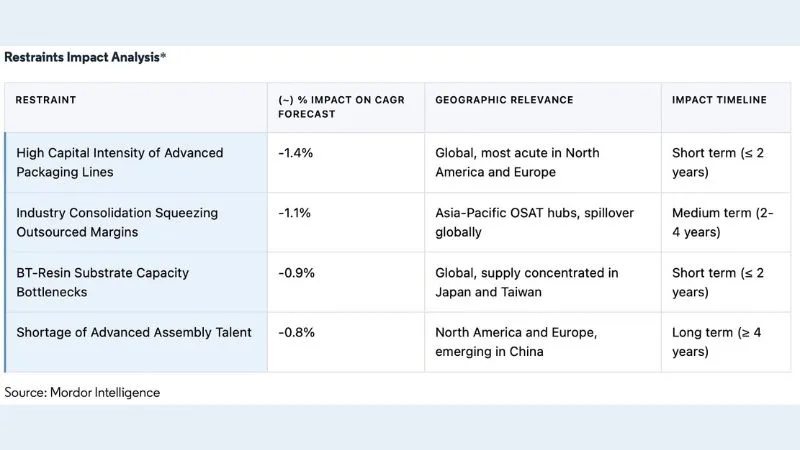
Industry Consolidation Squeezing Outsourced Margins
Integrated device manufacturers internalize packaging to guard chiplet interconnect IP, reducing third-party volume by double digits in 2025. Samsung bundles I-Cube packaging with foundry wafers, locking customers into single-vendor ecosystems. Amkor and ASE now compete on yield and lead time rather than price alone, yet shrinking customer pools compress negotiating latitude. Smaller OSATs struggle to fund next-generation lines, risking a drop in the number of viable suppliers below 10 by 2028, which could dampen innovation and elevate supply-chain risk.
Value Chain Analysis
The advanced packaging value chain begins with upstream materials, including substrates such as BT resin and ABF-related supply, copper and chemicals, underfill, and emerging glass-core formats. It then runs through equipment, including lithography, plating, bonding, metrology, and test, and into high-precision manufacturing spanning foundry-led advanced packaging and OSAT assembly and test, before ending with downstream integration into end products across consumer devices, data-center and HPC accelerators, and automotive power electronics.
Value capture is increasingly shaped by integrated platform offerings from large foundries and IDMs, including TSMC CoWoS and Intel Foveros, while OSATs such as ASE, Amkor, and Powertech compete on yield learning, cycle time, and co-design engagement for fan-out, SiP, and heterogeneous integration programs. Bottlenecks remain concentrated in high-end 2.5D/3D capacity and in enabling inputs, and they affect how value is captured across the chain. Industry commentary in 2026 also pointed to continued tightness in 2.5D packaging capacity amid AI-driven demand, reinforcing the importance of long-term capacity reservations and multi-sourcing across ASE, SPIL, and Powertech-type partners. TSMC’s 2026 scale-up across packaging facilities in Chiayi Science Park into mass production, alongside further site expansion, underscores how packaging capacity is being built via dedicated packaging campuses. As package power density rises, thermal-management materials and architectures are becoming higher-value steps in the chain, shifting differentiation toward materials innovation and advanced inspection and test rather than cost alone.
Competitive Landscape
Market structure is moderately consolidated, the top five vendors—Taiwan Semiconductor Manufacturing Company, Samsung Electronics, Amkor Technology, ASE Technology and Intel—commanded roughly 55% revenue in 2025, yet more than 20 additional companies remain active, preserving buyer flexibility. Each leading player bundles wafer fabrication with high-density interposer, fan-out or hybrid-bond capacity, capturing a premium for turnkey service that rivals cannot easily match. Samsung integrates I-Cube packaging with foundry wafers, locking customers into a single-vendor path that shields chiplet intellectual property and secures share in the advanced packaging market size.
Outsourced assembly and test providers face margin compression as integrated device manufacturers insource heterogeneous-integration lines. Amkor answers through geographic reach—Arizona for automotive, Portugal for aerospace—and by co-design partnerships that shorten time-to-yield for fabless designers. ASE Technology pairs its Siliconware joint venture with substrate expertise to guarantee supply during BT-resin shortages, a strategy that attracts graphics-processor clients hurt by 2024 material bottlenecks. Powertech Technology and JCET Group occupy specialist niches: automotive-qualified flip-chip for Powertech and fan-out panel-level modules for JCET, both contributing incremental advanced packaging market share while avoiding head-to-head combat with top-tier rivals.
Technology remains the core battlefront. TSMC owns more than 1 200 CoWoS patents, Intel leads copper-to-copper hybrid bonding, and Applied Materials dominates in glass-substrate equipment capable of 2 µm line-and-space resolutions. Start-ups focus on software: Ansys and Cadence extend electronic-design-automation flows that co-optimize multi-die power networks and thermal paths, lowering entry barriers for niche hardware innovators. Competitive intensity therefore hinges on capex scale, patent walls and ecosystem alignment, all of which propel continuous consolidation inside the advanced packaging market.
Source: Mordor Intelligence