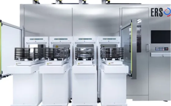
SUSS MicroTec SE has announced its official entry into the wafer-level cleaning sector with the introduction of its GreenTec Solutions product line and its inaugural cleaning system, the GT200.
The move expands SUSS’s semiconductor equipment portfolio into a wafer cleaning market valued at roughly €5.4 billion. Growth in this segment is accelerating due to rising demand for advanced packaging, heterogeneous integration, and artificial intelligence-driven high-performance computing (HPC) hardware.
“GreenTec Solutions marks an important milestone in the execution of our Ambition 2030 strategy,” said Burkhardt Frick, Chief Executive Officer of SUSS MicroTec. “By expanding into wafer-level cleaning, we are entering an attractive market with significant long-term growth potential while leveraging proven technologies and process expertise from our existing portfolio. Our differentiated approach combines strong cleaning performance, significantly lower chemical consumption, and the elimination of hazardous acids. This creates tangible benefits for customers and positions SUSS for future growth in advanced semiconductor manufacturing.”
Central to the new line is a hybrid cleaning architecture combining two field-proven technologies from the company’s Photomask Solutions division: TurbulenStrip and CrustBuster. TurbulenStrip blends lower-impact batch soaking with single-wafer handling to remove resist and chemical residues. Complementing it, CrustBuster uses patented in-situ ultraviolet (UV) technology inside a single-wafer chamber to decompose organic materials directly on the wafer surface. Working together, these tools deliver stable residue removal while cutting chemical consumption and helping chipmakers meet strict environmental, social, and governance (ESG) targets.
The GT200 is built for research and development, process qualification, and production across 200 mm manufacturing lines serving MEMS, RF, power devices, and CMOS applications. Alongside equipment deliveries, SUSS offers joint evaluation programs, process co-development, and recipe optimization to reduce integration risks ahead of volume production.
Looking forward, SUSS has outlined a clear path to high-volume manufacturing (HVM). Driven by customer demand, the company has pulled forward plans to release a dedicated 300 mm HVM platform in 2027, followed by a 200 mm HVM solution in 2028.
“We are building on decades of experience in demanding photomask applications and transferring this expertise now into eco-friendly wafer-level manufacturing,” noted Yuta Nagai, Senior Vice President Photomask Solutions at SUSS. Nagai added that early client interest prompted the company to advance its 300 mm roadmap to offer a seamless transition from pilot evaluation to full-scale fabrication.