Longtime display equipment maker Shindo Eng. Lab is moving into the semiconductor industry. Facing a slowing domestic display market and fierce global competition, the South Korean firm is using its display-making expertise to solve tough challenges in advanced chip packaging. The company has signed initial agreements with about 10 firms and is planning joint work with a major Taiwanese substrate maker.
As artificial intelligence and powerful computer chips run hotter, traditional plastic-like circuit boards tend to bend, warp, and hit physical limits. Glass substrates have emerged as a promising fix because they stay flat and sturdy. However, handling glass without cracking it or causing electrical defects remains difficult.
To solve this, Shindo Eng. Lab created Through Glass Ceramic Via (TGCV) technology. Instead of regular glass, it blends glass with ceramic. This special blend expands and contracts at a rate much closer to silicon chips and internal copper wires when heated, stopping tiny cracks from forming. The ceramic mix is also stiffer than standard glass, allowing factories to make thinner boards that take less time and metal to wire up.
The company is also adapting its display printing tools to make tiny electrical connection holes, called vias. Instead of using a slow laser to drill one hole at a time, it uses light and patterned masks to print millions of holes across an entire sheet at once. This method speeds up factory output and keeps every hole identical. Eleven global companies in the automotive, display, and materials sectors have already requested test samples.
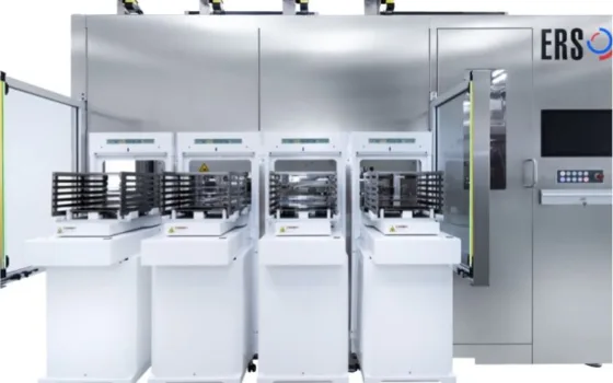
Beyond substrate materials, Shindo Eng. Lab’s precision vacuum bonding tools are attracting chipmakers. Overseas partners are testing its bubble-free lamination systems to hold delicate wafers securely during backend manufacturing for High-Bandwidth Memory (HBM) and next-generation optical chips.
“Advanced semiconductor packaging technologies like glass substrates are very similar to what we did in the display sector,” said Park Woong-ki, CEO of Shindo Eng. Lab. “The equipment tools we built over 30 years can be directly applied to microchips.”
With research staff making up roughly half of its 100-person team, the company aims to use this packaging expansion as a stepping stone into broader markets, including miniature sensors and wireless communication parts.