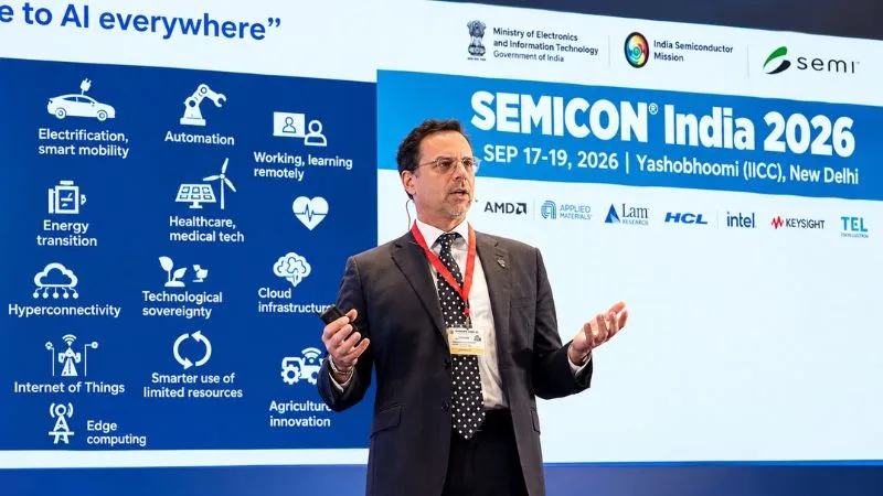
Lithography giant ASML has showcased its advanced, holistic lithography portfolio at SEMICON India 2026 in New Delhi, underscoring its role in establishing India’s commercial wafer fabrication infrastructure. As the sole global manufacturer of critical extreme ultraviolet lithography systems and a dominant force in deep ultraviolet tooling, the Dutch equipment manufacturer is focusing its technical and operational expertise on supporting high-volume silicon manufacturing within the country.
At the industrial level, lithography represents the most capital- and process-intensive stage of semiconductor front-end manufacturing. The precision patterning of nanometer-scale circuitry onto silicon wafers dictates overall transistor density, device speed, and power efficiency. At its SEMICON showcase, ASML detailed an integrated architecture combining:
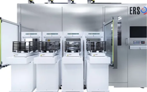
- High-productivity lithography exposure scanners
- Computational lithography software suites for pattern correction and defect modeling
- Inline optical and electron-beam metrology alongside high-speed wafer inspection
This closed-loop framework allows foundry engineers to identify micron-level patterning deviations in real time, accelerate process optimization, maximize silicon yield curves, and reduce ramp-up cycles from tool installation to commercial volume output.
Beyond hardware deployment, the company is solidifying local operational roots. Following a Memorandum of Understanding signed in May 2026 with Tata Electronics, ASML is directly assisting the buildout and tool ramp-up of India’s premier 300 mm commercial semiconductor fabrication facility in Dholera, Gujarat. To support this fab and regional customers, ASML has incorporated a domestic legal entity and is establishing a dedicated customer support and engineering office in India.
Speaking at the NEXTGEN Manufacturing Forum, Wayne Allan, Executive Vice President and Chief Strategic Sourcing & Procurement Officer at ASML, stressed the necessity of deep ecosystem alignment across equipment supply chains, research institutions, and fabrication sites.
The industrial timing coincides with the massive hardware demands of Artificial Intelligence workloads. Modern AI accelerators require ultra-dense packaging and tightly controlled lithographic tolerances to manage memory-to-logic interconnects and thermal loads. ASML’s integrated metrology and computational lithography toolsets allow domestic fabs to manufacture complex logic and memory chips with the tight process windows required by AI applications.
Through system installations, local supply chain readiness initiatives, and specialized workforce training, ASML’s expanding technical footprint is accelerating India’s transition from chip design leadership into large-scale, high-yield wafer manufacturing.