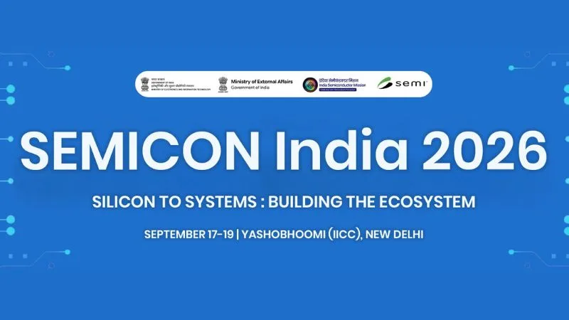
Prime Minister Narendra Modi will inaugurate the fifth edition of SEMICON India 2026 on September 17 at Yashobhoomi in Dwarka, New Delhi. Organized under the theme “Silicon to Systems: Building the Ecosystem,” the three-day flagship conference convenes over 600 exhibitors including 300 international firms and 150 industry leaders across 15,000 square meters. The summit represents a strategic transition from policy incentives to active commercial execution across the global semiconductor matrix.
Expanding Domestic Manufacturing and Fiscal Support
India’s semiconductor ambitions build directly on its high-volume electronics manufacturing base. Domestic electronics output surged from ₹1.9 lakh crore in FY 2014–15 to ₹13.11 lakh crore in FY 2025–26, during which exports reached ₹4.24 lakh crore. In the same period, mobile phone production grew to ₹6.27 lakh crore, with exports totaling ₹2.59 lakh crore, elevating smartphones to India’s leading single export commodity.
To capture the foundational silicon value layer, the Union Cabinet augmented its initial ₹76,000 crore outlay by approving Semicon India Programme 2.0 with a dedicated commitment of ₹1,27,500 crore. The updated industrial blueprint addresses six integrated pillars:
- Silicon and compound semiconductor fabrication facilities
- Advanced packaging, testing, and OSAT (Outsourced Semiconductor Assembly and Test)
- Semiconductor equipment manufacturing and specialty materials
- Chip design and Intellectual Property (IP) creation
- Focused research and development (R&D)
- High-volume workforce and engineering talent pipelines
Twelve semiconductor projects across six states have received formal approval, representing over ₹1.64 lakh crore in committed capital. Three facilities have already commenced commercial production, establishing operational manufacturing on the ground.
Architecture, EDA Access, and Sub-Micron Nodes
Beyond fab floor infrastructure, India is advancing its front-end electronic design automation (EDA) and tape-out capacity through the Chips to Startup (C2S) program and the Design Linked Incentive (DLI) scheme:
- EDA Tool Deployment: Deployed across 320 academic institutions, with 105 startups and MSMEs receiving subsidized access to industrial design suites.
- ChipIN Infrastructure: Hosted at C-DAC, the ChipIN Centre provides shared compute, verification, and foundry interfaces for over 100,000 engineers across 500 organizations, accumulating over four crore tool usage hours.
- Tape-Out Velocity: By April 2026, 75 institutions successfully taped out 211 silicon chips. Seven architectures reached tape-out down to advanced 12-nanometer nodes for fabrication via domestic and overseas foundries.
- Workforce Target: Structured training tracks have engaged more than 68,000 students to date toward a target of 85,000 specialized semiconductor engineers by 2030.
Multilateral Alignment and AI Integration
Global supply disruptions during recent crises highlighted the vulnerability of single-source production corridors. In response, India formally acceded to the Pax Silica coalition at the India AI Impact Summit 2026. The multilateral agreement secures end-to-end silicon workflows—ranging from critical mineral access and precision lithography to foundational AI accelerators and edge deployment infrastructure.
By linking domestic fabrication, packaging, and EDA capabilities with strategic international partnerships, India is establishing long-term technological sovereignty across the global silicon supply chain.