Global Unichip Corp. (GUC) has confirmed that its High Bandwidth Memory 4E (HBM4E) Physical Layer (PHY) and Controller IP is silicon-ready, securing immediate adoption within tier-one customer AI ASICs. Fabricated on TSMC’s cutting-edge N2P nanosheet process node, the test vehicle achieved physical tape-out using TSMC’s Chip-on-Wafer-on-Substrate with Local Silicon Interconnect (CoWoS-L) packaging technology.
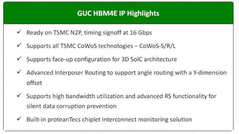
The tape-out marks an important manufacturing milestone for heterogeneous compute clusters. Building upon GUC’s volume-proven 12 Gbps HBM4 portfolio on the N3P node, the updated HBM4E IP raises deterministic data transfer rates to 16 Gbps across all corner PVT (process, voltage, temperature) timing sign-offs.
To overcome severe signal degradation and crosstalk at 16 Gbps, GUC deployed proprietary interposer routing schemes capable of handling non-orthogonal angle traces with Y-dimension offsets. This layout co-optimization directly secures Signal Integrity (SI) and Power Integrity (PI) targets across all CoWoS implementations, including silicon interposers (CoWoS-S), redistribution layer substrates (CoWoS-R), and bridge-die configurations (CoWoS-L).
For high-density 3D heterogeneous stacking, GUC introduced a specialized face-up PHY variant tailored for TSMC’s SoIC-X (System-on-Integrated-Chips with direct copper-to-copper bonding) platform. Serving as a bottom base die, it features dedicated Through-Silicon Vias (TSVs) for vertical signal extraction and low-loss feedthrough power rails to top compute dies, bypassing traditional microbump thermal and parasitic limits.
To ensure manufacturing yield and field reliability, the design embeds proteanTecs’ on-chip interconnect monitoring telemetry. This enables deep structural diagnostics across chiplet microbumps during automated testing (ATE) while providing runtime fleet tracking. The controller also incorporates hardware-level Reed-Solomon (RS) error-correcting codes to stop silent data corruption (SDC).
“Reaching 16 Gbps on TSMC’s N2P process underscores GUC’s ability to quickly turn leading-edge process and packaging technology into production-ready HBM solutions,” said Igor Elkanovich, Chief Technology Officer of GUC. “By uniting our face-up HBM, face-up UCIe, and GLink-3D IPs, GUC delivers a complete interface IP portfolio for 3D SoIC architectures.”