Samsung Electronics has entered a strategic technology partnership with Mistral to integrate specialized computational infrastructure across its semiconductor engineering and manufacturing lines. Formalized during a bilateral state summit between South Korea and France in Paris, the agreement pairs Samsung’s silicon fabrication capacity with localized enterprise models, supported by Samsung leading Mistral’s Series D funding round to acquire an equity stake.
As advanced fabrication transitions through gate-all-around (GAA) logic architectures and high-density memory topologies like High Bandwidth Memory (HBM) and multi-layer 3D NAND, process margins have narrowed to atomic scales. Modern fabrication facilities generate petabytes of daily telemetry from deep-ultraviolet (DUV) and extreme-ultraviolet (EUV) lithography scanners, plasma etch chambers, and chemical-mechanical planarization (CMP) stations. Analyzing this telemetry quickly enough to correct drifting process recipes before wafers suffer critical yield degradation has become a primary operational challenge.
Under the agreement, Samsung will implement on-premises software deployments powered by Mistral Large across its Device Solutions (DS) division, spanning logic foundries and memory lines. On-premises containment is a critical engineering prerequisite for semiconductor production. Because wafer recipes, optical proximity correction (OPC) data, reticle parameters, and physical mask layouts constitute proprietary intellectual property, all data processing, equipment diagnostics, and automated process adjustments will remain strictly isolated within Samsung’s internal firewall infrastructure.
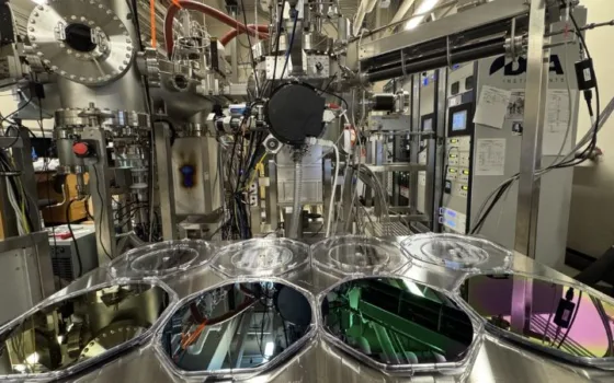
On the cleanroom floor, the platform will process inline sensor logs and metrology imagery to accelerate defect classification, automate tool parameter calibration, and stabilize yield learning curves. Instead of relying solely on post-exposure optical inspection runs, tools can dynamically flag anomalous process signatures—such as chamber pressure fluctuations, temperature gradients, or RF power drifts in plasma reactors—mitigating structural micro-defects before whole lots suffer irreversible wafer scrap.
“Increasing complexities involved in chip design and manufacturing require continuous innovation in semiconductor technologies,” said Young Hyun Jun, Vice Chairman and CEO of Samsung Electronics’ DS Division. “We look forward to working with Mistral and supporting the evolving needs of customers, while delivering breakthroughs essential to the industry.”
Arthur Mensch, co-founder and CEO of Mistral, highlighted the alignment between hardware execution and algorithmic workflows, “We are proud to support Samsung Electronics with our technical expertise, helping to improve how chips are designed and manufactured, and to accelerate technical progress across the global value chain.”
The collaboration establishes an automated closed-loop architecture linking front-end wafer fabrication, advanced packaging workflows, and foundry contract manufacturing. By embedding real-time predictive data pipelines directly into its cleanrooms, Samsung aims to compress engineering ramp cycles, stabilize critical etch and deposition processes, and protect manufacturing margins at leading-edge nodes.