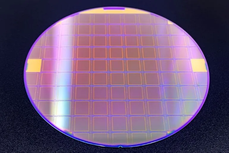
Japan-based Sumitomo Chemical Co., Ltd. has officially started mass production of four-inch Indium Phosphide (InP) epitaxial wafers, aiming to address the fast-growing hardware demands of artificial intelligence data centers and high-speed optical communication networks.
As one of the select few semiconductor materials suppliers in Japan capable of stably manufacturing InP epiwafers at scale, the company has set an ambitious commercial target. It expects to generate approximately ¥10 billion in annual sales from its new InP wafer business by the mid-2030s.
The global boom in generative artificial intelligence, coupled with the rapid expansion of cloud computing, the Internet of Things (IoT), and high-capacity telecommunications, has placed severe pressure on modern computing infrastructure. Data centers worldwide are currently handling unprecedented volumes of information, leading to steep increases in power consumption, heat generation, and network latency.
To overcome these physical bottlenecks, the technology industry is increasingly turning to photonic-electronic convergence—an architectural approach that uses light rather than traditional electrical signals to transmit data faster and with far greater energy efficiency. Within this technological shift, Indium Phosphide epiwafers serve as a foundational semiconductor substrate for manufacturing high-performance lasers, optical transceivers, and advanced optoelectronic components.
Producing commercial-grade InP epiwafers is technically demanding. The manufacturing process requires ultra-precise control over crystalline composition, high-temperature epitaxial growth, and surface smoothness. In addition, manufacturers must maintain strict quality control and sophisticated safety protocols when managing precursor gases and complex chemical reactions.
Sumitomo Chemical successfully established its mass-production setup by leveraging more than twenty-five years of research and manufacturing expertise gained from producing Gallium Arsenide (GaAs) and Gallium Nitride (GaN) wafers. By combining its proprietary crystal growth techniques, thin-film stacking methods, and composition control, the company has achieved high yields and uniform wafer quality suitable for tier-one component makers.
The launch of InP epiwafers marks another key milestone in the company’s broader corporate strategy. Sumitomo Chemical has identified its Information and Communication Technology (ICT) & Mobility Solutions segment as a primary growth driver, with semiconductor materials at the center of its long-term expansion plans.
With this commercial rollout, Sumitomo Chemical broadens its compound semiconductor portfolio, which already features high-purity GaN substrates, GaN epiwafers, and GaAs epiwafers. Looking ahead, the company plans to deepen its presence in key high-growth markets, including next-generation wireless communications, automotive power electronics, and hyperscale data center infrastructure.