The Union Government has officially notified the Semicon 2.0 scheme with an expanded financial outlay of ₹1.27 lakh crore. The comprehensive policy framework is designed to provide sustained financial and infrastructural support across the entire semiconductor value chain, advancing India’s goal of building a self-reliant and globally competitive electronics manufacturing base.
Building upon the progress achieved under the first phase of the Semicon India Programme, the new framework expands its focus beyond basic chip fabrication. It introduces structured fiscal incentives across six core pillars: indigenous chip design, semiconductor equipment and machinery, new commercial fabrication plants, outsourced semiconductor assembly and test (OSAT) and advanced packaging units, research and development, and specialized talent development.
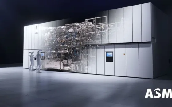
Under the notified guidelines, the government will provide central fiscal support of up to 40% of capital expenditure for setting up commercial silicon wafer fabs with a minimum investment threshold of ₹20,000 crore. Compound semiconductor, photonics, sensor, and display fabrication projects will be eligible for 35% capex support. To encourage the development of local equipment and raw materials, the policy offers 30% capital support alongside production-linked incentives ranging from 2% to 10% for equipment manufacturing. Advanced packaging and ATMP facilities will receive support of up to 35%, while research initiatives can secure grants covering up to 75% of project costs.
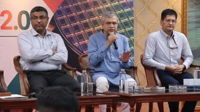
Addressing the media, Union Minister for Electronics and IT Ashwini Vaishnaw highlighted that the initiative aims to make India an essential partner in the global supply chain over the coming decades. He noted that the domestic ecosystem is projected to attract investments exceeding ₹4 lakh crore and generate between 50,000 and 60,000 direct high-technology jobs. A high-level expert panel, co-chaired by the Principal Scientific Adviser and the National Security Adviser, will identify critical semiconductor products to ensure strategic self-reliance in vital areas such as compute, RF, power electronics, and sensors.
The India Semiconductor Mission (ISM) will serve as the nodal agency responsible for appraising applications, coordinating with industry stakeholders, and overseeing project execution. The application window will initially remain open for three years, with individual project support extending up to six years. The initiative also places strong emphasis on training one lakh additional semiconductor design engineers to support long-term industry expansion.