South Korea’s fabless and semiconductor design ecosystem is stepping onto the global stage at IFA 2026 in Berlin, Germany. Organized by the National IT Industry Promotion Agency (NIPA), the K-AI Semiconductor Pavilion features 12 domestic enterprises and research institutions presenting commercial-grade silicon architectures, custom accelerators, and real-world deployment frameworks from September 4 to 8 at Messe Berlin.
Hardware Architectures and Edge Computing Focus
Located at Hall 5.2b, Stand 400, the pavilion highlights South Korea’s transition from high-volume memory fabrication toward custom logic, edge processing, and high-efficiency compute engines. While global hardware demand has long centered on monolithic graphics processing units (GPUs) for hyperscale cloud training, the engineering exhibits emphasize application-specific integrated circuits (ASICs) and dedicated Neural Processing Units (NPUs).
These specialized silicon architectures target the growing computational demands of inference workloads. By optimizing data path execution and tailoring memory bandwidth for low-latency matrix operations, modern NPUs achieve high compute density within constrained thermal design power (TDP) envelopes. Demonstrations at the pavilion focus heavily on edge and on-device computing platforms, where low power consumption, deterministic response times, and localized data processing are critical design criteria.
Industrial Integration and Domain-Specific Silicon
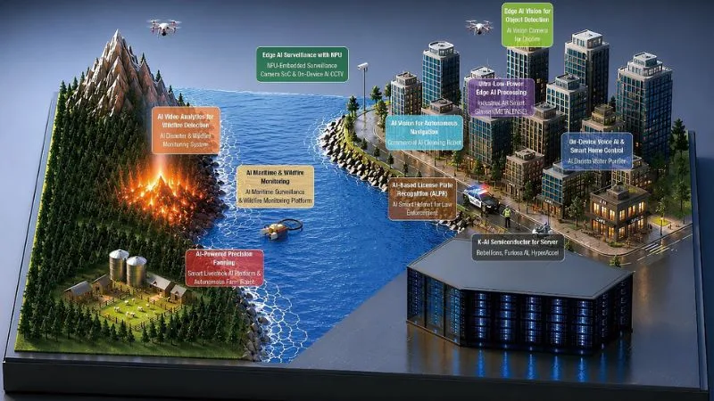
Rather than treating semiconductor designs solely as standalone components, the showcase demonstrates how domestic processors integrate directly into industrial automation, intelligent transportation systems, robotics, and smart city infrastructure.
In robotics and autonomous mobility, deterministic hardware accelerators handle multi-sensor fusion, image processing, and simultaneous localization and mapping (SLAM) directly at the device level. By eliminating round-trip latency to cloud data centers, these edge-compute chips enable fail-safe operation for industrial automated guided vehicles (AGVs) and machine vision systems on factory floors. Similarly, in public safety and infrastructure monitoring, on-device vision processing units (VPUs) execute localized object detection and anomaly alerts while maintaining data privacy and reducing transmission bandwidth.
Commercialization Pathways and International Sourcing
NIPA, a state-backed agency tasked with expanding South Korea’s ICT infrastructure and global commercial footprint, has tailored the pavilion to bridge the gap between initial tape-out, silicon validation, and commercial adoption. Historically, fabless design houses face significant hurdles in moving past engineering samples to secure tier-one international design wins and production scaling.
To accelerate design-in cycles and cross-border partnerships, the pavilion will host K-AI Connect, an executive networking reception scheduled for September 6 from 16:00 to 18:00. The session provides an interface between Korean chip designers, global system integrators, original design manufacturers (ODMs), and international component distributors.
As worldwide industrial sectors integrate localized compute into edge endpoints, the hardware demands on latency, silicon footprint, and power efficiency continue to tighten. The K-AI Semiconductor Pavilion underscores South Korea’s strategic engineering push to diversify its semiconductor footprint, moving beyond commodity memory chips into competitive, domain-specific accelerator silicon for the international hardware supply chain.