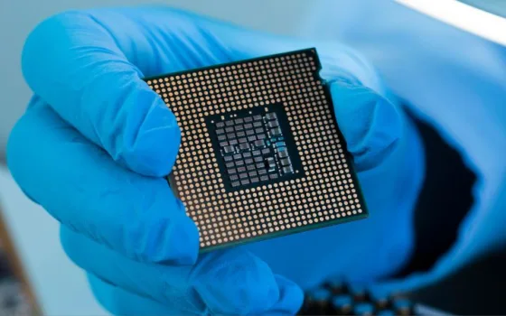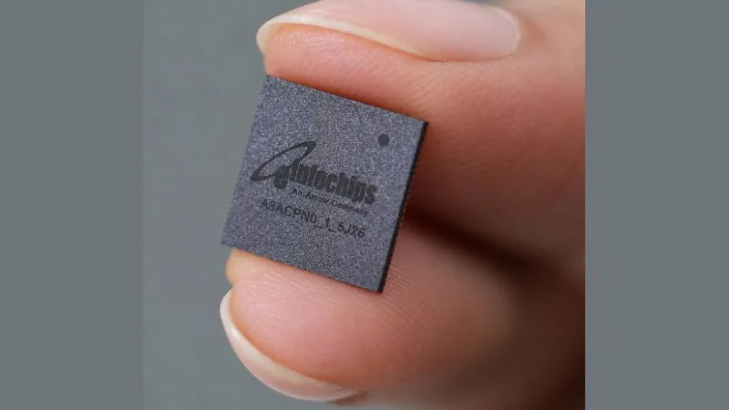
eInfochips, an Arrow Electronics company, has demonstrated its end-to-end turnkey ASIC design capabilities by executing the complete development, fabrication, packaging, and post-silicon bring-up of an integrated test chip. The tape-out and physical validation mark a significant milestone for the engineering services provider, establishing its operational transition from discrete front-end design support to full-lifecycle silicon execution.
The physical test chip architecture integrates a dedicated microcontroller core alongside embedded circuitry configured for real-time current and voltage monitoring, software-defined programmability, on-chip diagnostics, and system protection. By condensing multi-component power sensing, telemetry, and control logic onto a unified silicon die, the design eliminates peripheral discrete chips and simplifies board-level printed circuit layout. This monolithic approach reduces Bill of Materials (BOM) complexity while enhancing measurement accuracy, fault protection, and system-level responsiveness for space-constrained electronics.
Developing proprietary application-specific integrated circuits presents significant operational hurdles for system OEMs, automotive tier-ones, and industrial equipment builders. Navigating custom silicon traditionally requires handling multiple fragmented vendor relationships, managing separate handoffs between digital RTL designers, third-party IP vendors, pure-play wafer foundries, OSAT assembly houses, and test engineering labs. Sumit Sethi, Vice President and General Manager of Engineering Services at eInfochips, pointed out that coordinating across these dispersed ecosystem partners introduces execution friction and technical risk. Taking turnkey ownership allows design service firms to mitigate multi-vendor handoffs, unify accountability, and compress the cycle time from initial architecture to verified silicon.
The demonstration leverages eInfochips’ background supporting automotive, industrial, and semiconductor engineering programs. Its capabilities span the semiconductor stack, encompassing microarchitecture, intellectual property implementation, analog and mixed-signal blocks, design for testability (DFT), physical implementation, golden sign-off, post-silicon electrical characterization, and foundry ecosystem logistics. As systems enterprises increasingly develop bespoke processors to secure hardware differentiation, reliable turnkey access to fabrication and backend assembly has become a critical requirement.
This milestone reflects a broader structural realignment within global semiconductor supply chains. Tier-one electronic distributors and engineering service providers are moving higher up the silicon value chain, serving as vital aggregators between fabless startups, non-traditional chip developers, and major contract manufacturing partners. With market demand shifting toward custom silicon across industrial automation, edge devices, and electric vehicles, end-to-end turnkey engineering platforms lower the barrier to silicon ownership, providing an established pathway to tape-out and volume qualification without requiring captive internal fabless organizations.