Both Intel Foundry and ASML have recently made important announcements during the SPIE Photomask Technology + Extreme Ultraviolet Lithography event about their plans for making high NA EUV lithography commercially viable. Both firms addressed issues relating to practical manufacturing progress, today’s chip designs, and future efforts to redefine mask standards for semiconductor manufacturing.
Manufacturing Milestones and Panther Lake Progress
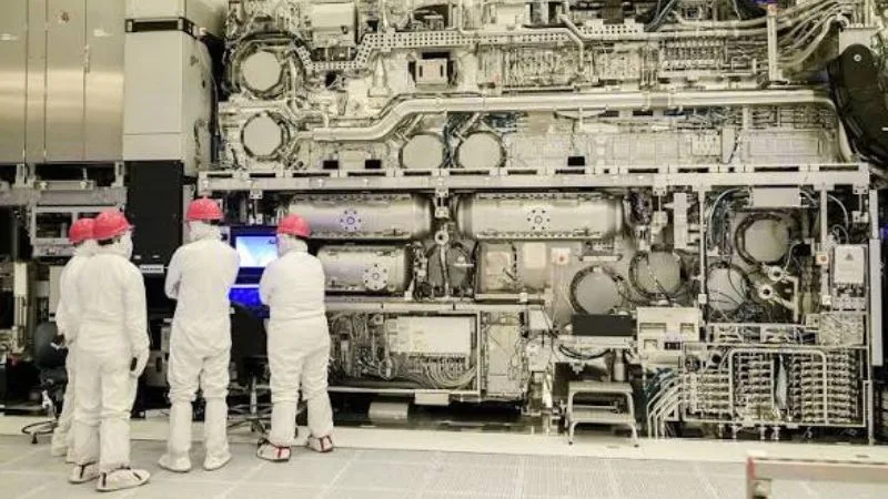
The Intel Foundry has now successfully installed the High NA EUV technology in its operational manufacturing line. Over a million wafers have been manufactured using this technology through early equipment validation, research and development, and production of selected layers in Intel’s future generation of the Core Ultra Series 3 processors named as the Panther Lake. Metrics such as equipment availability, wafer production efficiency, and overlay accuracy have been performing in line with Intel’s objectives.
Semiconductors manufactured using the Intel 18A process node with high-NA EUV for certain layers are performing similarly or better than the same layers manufactured using low-NA EUV technologies, the NXE family of tools.
Current Mask Strategy and Reticle Stitching
A primary challenge with High NA lithography is its half-field exposure size, which cuts the maximum printable area on a standard reticle in half. To work around this limitation without forcing customers into immediate ecosystem redesigns, Intel Foundry is utilizing two distinct paths on current 6-inch masks:
- Floor-Planning: Designing smaller chips or functional blocks that fit entirely within the native half-field size of a High NA exposure.
-
Reticle Stitching: Splitting large chip patterns across two exposures on a standard 6-inch mask and joining them seamlessly on the wafer using Process Design Kit (PDK) solutions.
During the conference, speakers from both organizations outlined technical requirements for this approach. Jan van Schoot from ASML detailed scanner alignment and mask specifications required for half-field exposure, while Kimberly Pierce from Intel Foundry presented real-world data on using reticle stitching in active production lines.
The Push for 6×12-Inch Masks
Whereas reticle stitching immediately offers a stopgap for existing semiconductor designs, Intel Foundry and ASML are encouraging the semiconductor industry to move towards a larger physical mask size. For more than three years now, Intel Foundry has been spearheading efforts towards the creation of the 6×12-inch mask standard.
Moving away from the old 6-inch square masks to rectangular 6×12-inch masks allows the high NA systems to perform full-field exposures again. Such a transition will need cooperation between different sectors of the industry:
- EDA Partners: Creation of design automation tools suitable for larger layout areas and new layout rules.
- Mask Manufacturers and Suppliers: Manufacturing of new substrate blanks, inspection systems, and handling systems for oversized masks.
- Automation & Material Partners: Modification of robotic systems, pods, and cleaning lines to fit the new sizes.
Intel Foundry and ASML have continued their collaboration with suppliers, automations, material firms, and rival chip producers to create formal specifications for 6×12 inch tools. The two-pronged approach helps chip designers access High NA tools through stitching of standard 6 inch mask while setting the stage for complete migration to 6×12 inch masks in the next generation manufacturing nodes.