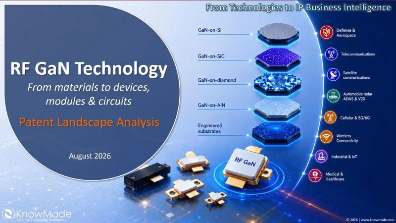
Radio-frequency gallium nitride (RF GaN) technology has transitioned into an aggressive phase of industrial growth and strategic intellectual property (IP) realignment, according to KnowMade’s RF GaN Technology Patent Landscape Analysis 2026. While 5G and telecommunications infrastructure have historically anchored the market, demand is surging in high-reliability aerospace, electronic warfare, counter-unmanned aerial systems (C-UAS), and satellite communications.
As global defense budgets expand, the sector faces extensive restructuring fueled by corporate consolidation, cross-border patent transfers, technology licensing, and national manufacturing-sovereignty mandates. At the same time, export restrictions on critical raw materials and proprietary process recipes are forcing manufacturers to secure verified, domestic supply chains.
KnowMade’s analysis identifies a clear structural shift: while overall patenting volume is stabilizing as core RF GaN technologies mature, competition is intensifying within specific substrate platforms and geographic jurisdictions. IP leadership is increasingly measured by patent portfolio breadth, multi-jurisdictional filings, and exclusive ownership of advanced manufacturing processes.
From a technology platform perspective, GaN-on-silicon carbide (GaN-on-SiC) remains the benchmark architecture for high-power radar, electronic attack payloads, and macro basestations. Its superior power density, high breakdown voltage, and proven thermal dissipation maintain its position as the standard for mission-critical deployments. However, industry adoption continues to grapple with steep barriers to entry, including limited semi-insulating SiC substrate availability, intricate epitaxy know-how, long military qualification timelines, and the slow migration toward 150mm and 200mm wafer formats.
Simultaneously, GaN-on-silicon (GaN-on-Si) is moving into commercial volume production, buoyed by the scale economics of 8-inch (200mm) CMOS-compatible silicon foundries. GaN-on-Si presents an attractive cost profile for lower-power RF architectures and emerging sub-THz, FR3, and early 6G bands operating above 10 GHz. Nonetheless, industrial uptake must still overcome mechanical challenges like lattice mismatch, substrate warping, thermal dissipation limits, and long-term device reliability.
Looking further ahead, R&D groups are aggressively filing patents around wide-bandgap alternatives, including GaN-on-diamond and GaN-on-aluminum nitride (AlN). Although high substrate synthesis costs and integration complexities keep them in exploratory stages, early patent portfolios reflect an effort to solve ultimate thermal bottlenecks.
Geographically, regional IP portfolios show distinct industrial specializations:
Japan: Companies maintain strong leverage across upstream materials. Sumitomo Electric and NGK Insulators lead in GaN substrates and epiwafers, while Shin-Etsu has emerged as an active challenger.
United States: American firms dominate downstream devices and integrated circuits. Following its acquisition of Wolfspeed’s RF business, MACOM has secured a leading end-to-end IP footprint across discrete devices, monolithic microwave integrated circuits (MMICs), and packaging architectures.
China: Domestic activity remains led by research institutes like CETC and Xidian University, though commercial players such as Huawei, Enkris, and Hanhua Semiconductor are rapidly expanding their private IP holdings.
With companies aggressively extending patent families across the US, Europe, and Asia, patents have become essential instruments to safeguard manufacturing routes, retain freedom to operate, and dictate terms in future technology licensing agreements.
Source: KnowMade (RF GaN Technology Patent Landscape Analysis 2026)