In a major breakthrough for sub-5-nanometer semiconductor scaling, a research team led by Prof. REN Wencai from the Institute of Metal Research (IMR) of the Chinese Academy of Sciences has successfully achieved the wafer-scale epitaxial growth of monolayer MoSi2N4 single crystals. The high-performance p-type two-dimensional (2D) semiconductor marks a vital step toward realizing complementary metal-oxide-semiconductor (CMOS) logic architectures built entirely from atomically thin materials. The study was published in Nature Materials
As traditional silicon transistors approach fundamental physical boundaries, chip designers face severe short-channel effects, excessive leakage currents, and thermal dissipation limits. Atomically thin van der Waals layered 2D materials, featuring dangling-bond-free surfaces, offer a compelling pathway to bypass these roadblocks below the 5-nanometer node. While n-type 2D semiconductors like MoS2 and WS2 have previously attained wafer-scale single-crystal status, matching p-type materials with high carrier mobility and environmental stability have remained exceptionally elusive.
This material breakthrough arrives at a critical juncture for artificial intelligence compute infrastructure. Modern AI clusters and deep-learning accelerators demand unprecedented transistor density and ultra-low switching power to process massive neural networks. By enabling true 2D CMOS logic, p-type 2D crystals like MoSi2N4 provide the essential foundation needed to construct dense, energy-efficient AI processors that avoid the thermal choking and standby power drain plaguing advanced silicon nodes.
The IMR team initially pioneered the MoSi2N4 structure in 2020 by introducing silicon into a molybdenum nitride system, inaugurating the MA2Z4 family of layered materials. While monolayer MoSi2N4 demonstrated a bandgap comparable to MoS2 alongside superior theoretical carrier mobility, thermal conductivity, and mechanical strength, previous synthesis methods were limited to polycrystalline films. Random grain boundaries scattered charge carriers and tore films during device transfer.
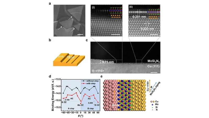
To resolve this bottleneck, the researchers designed a customized chemical vapor deposition (CVD) process utilizing Cu(111) single crystals pre-enriched with molybdenum and silicon atoms. Atomic <110> steps across the copper substrate guided the unidirectional nucleation of MoSi2N4 domains. Because each domain shared identical crystal orientation, they stitched seamlessly together into a continuous, defect-suppressed single crystal.
The grown monolayer MoSi2N4 exhibits an intrinsic carrier mobility of 154 cm² V⁻¹ s⁻¹. Integrated field-effect transistor (FET) arrays fabricated from the single-crystal layer recorded an on/off current ratio of 3.8 ± 1.4 × 10⁶ and an on-state current density reaching 17.96 μA μm⁻¹ at a 1-micrometer channel length. Furthermore, the devices demonstrated superior operational stability over standard monolayer WSe2 alternatives.
The research team confirmed the versatility of this epitaxial approach by successfully growing wafer-scale monolayer WSi2N4 single crystals as well. Beyond delivering a viable p-type platform for 2D CMOS integration, this scalable growth protocol establishes a reproducible blueprint for synthesizing a wide class of next-generation 2D materials for advanced nanoelectronics.