Advanced packaging equipment specialist Manz Asia has entered into a strategic collaboration with semiconductor process solutions provider SUSS to co-develop next-generation industrial inkjet printing technology. The initiative targets advanced packaging and high-density semiconductor fabrication lines, aiming to transition digital printing from process research and development into automated, high-volume manufacturing (HVM).
Industrial Context and Additive Coating Drivers
As backend semiconductor manufacturing transitions toward heterogeneous integration, larger-format substrates, and multi-die topologies, conventional spin-coating and slit-die coating methods encounter physical and economic limits. Traditional approaches often suffer from high material waste—spinning off significant volumes of costly polymer dielectrics and passivation layers—while struggling with uniform edge-bead control and topography conformal coverage on large substrates.
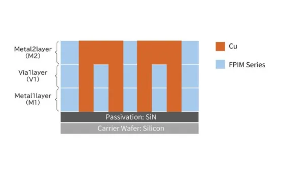
Industrial inkjet printing provides an additive, maskless alternative. By depositing functional fluids and specialty materials with picoliter-level droplet precision exclusively where required, inkjet architectures dramatically minimize chemical consumption, eliminate discrete masking and etching phases, and streamline overall process routing. These technical efficiencies make the technology especially suited for complex topologies, wafer reconstitution, and tall copper-pillar structures common in multi-die chip architectures.
Integrating Engineering and Process Ecosystems
The collaboration bridges complementary capabilities between the two equipment builders. Manz Asia contributes specialized automation, established hardware integration, and industrial expertise across the panel-level packaging (PLP) ecosystem. The company’s proprietary “Lab-to-Fab” framework encompasses substrate surface pre-treatment, chemical handling, precise jetting, thermal curing, and in-line metrology characterization.
SUSS contributes global market reach and deep institutional knowledge in semiconductor backend lithography, wafer bonding, and specialized coating solutions. Together, the engineering teams will optimize droplet-surface interaction dynamics, validate novel dielectric formulations, and establish rigorous quality criteria to shorten time-to-market for production-ready toolsets.
Expanding Into Panel-Level Packaging
The partnership places specific emphasis on accelerating adoption within fan-out panel-level packaging (FOPLP). Shifting fabrication from standard 300 mm round silicon wafers to large rectangular panels maximizes operational area efficiency and throughput, which is vital to reducing the cost of complex packaging for computing workloads.
“Successfully commercializing new semiconductor technologies requires deep process expertise, strong application know-how and close alignment with customer roadmaps,” stated Burkhardt Frick, CEO of SUSS. “By combining SUSS’ semiconductor process experience with Manz Asia’s inkjet expertise, we can accelerate technology development and reduce time-to-market for future solutions. At the same time, the collaboration strengthens our access to the emerging panel-level packaging ecosystem… supporting our Ambition 2030 strategy.”
Robert Lin, CEO of Manz Asia, highlighted the structural evolution underway in backend packaging: “Panel-level packaging is entering a new phase, driven by higher integration and increasingly complex structures. These developments are creating new demands for greater process flexibility, material efficiency and manufacturing scalability. Through our collaboration with SUSS, Manz Asia is combining its inkjet printing and manufacturing expertise with SUSS’ semiconductor process capabilities and global customer reach to deliver scalable, next-generation solutions.”
By aligning material qualification, deposition hardware, and production-line engineering, both companies intend to provide foundry, OSAT, and substrate manufacturers with a scalable path toward high-efficiency additive packaging lines.