

The global semiconductor landscape is witnessing a structural transformation. As artificial intelligence radically challenges conventional microarchitectures, the era of relying solely on general-purpose compute is making way for heterogeneous, workload-specific silicon. In this shifting paradigm, the true measure of innovation is no longer sheer processor size, but power efficiency, latency, data movement, and purpose-built edge acceleration. For India, this disruption offers a historic opening—one where strategic design, intellectual property (IP) creation, and agile engineering execution can catalyze semiconductor sovereignty faster and more sustainably than capital-intensive fabrication alone.
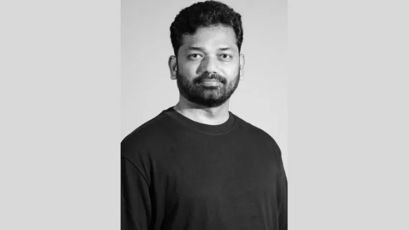
In a recent interaction with Rashmi Verma, Suresh Babu Katta, Founder & CEO, Nanopowered Technologies, discussed how India must transition from being an engineering execution back-office into a powerhouse of proprietary silicon IP and product ownership. Highlighting the critical need for patient early-stage capital, higher risk appetite, and domestic reusable IP, he emphasized that cultivating end-to-end engineering talent—bridging system architecture to silicon validation—is essential for long-term competitiveness. Pointing to Nanopowered’s strategic roadmap, Katta outlined how agile startups can carve defensible niches across critical signoff, edge AI, and application-specific domains to meet evolving global OEM expectations.
How is AI fundamentally altering microarchitecture decisions, and where are the opportunities for purpose-built silicon?
AI is fundamentally changing the way we think about processor architecture. The traditional approach was to build increasingly powerful general-purpose processors and rely on software to extract performance. AI workloads are challenging that model because they are dominated by highly parallel computation, large data movement, memory bandwidth, and increasingly stringent power constraints.
We are therefore seeing a shift towards heterogeneous and workload-specific architecturescombining CPUs with NPUs, GPUs, DSPs and dedicated accelerators. The key microarchitectural decisions are no longer only about compute performance; they are equally about performance per watt, memory hierarchy, data movement, latency and determinism.
We see a particularly compelling opportunity at the edge. Edge AI devices cannot afford the power, latency or connectivity requirements of sending every workload to the cloud. Purpose-built silicon for vision, industrial automation, automotive, security, smart cameras, wearables and intelligent consumer electronics can deliver much better efficiency by moving computation closer to the data.
The next phase of semiconductor innovation will therefore not necessarily be about building the biggest processor. It will be about building the right silicon for the right workload.
Why is chip design uniquely positioned to drive India’s semiconductor breakthrough faster than manufacturing alone?
Manufacturing is unquestionably critical to semiconductor sovereignty, but design is where India can create value and intellectual property much faster.
India already possesses one of the world’s largest pools of semiconductor engineers and has decades of experience in digital design, verification, physical design, embedded systems and chip implementation. This gives us a significant starting advantage.
A fab requires enormous capital, infrastructure, utilities, process technology and years of execution before it reaches scale. A fabless design company, by contrast, can leverage global foundries and focus its capital on architecture, IP, design, software and product innovation.
The real opportunity is to move up the value chain from being an engineering execution centre to becoming an IP and product creation centre.
If India can create globally relevant semiconductor IP and fabless products, every successful design can potentially be manufactured at multiple foundries and sold across international markets. That creates a multiplier effect.
So, the objective should not be design versus manufacturing. It should be design + IP + manufacturing + packaging + software + products. Design can provide the fastest route to building indigenous intellectual property and globally scalable semiconductor businesses while the manufacturing ecosystem develops in parallel.
What structural shifts are needed for India to build enduring global semiconductor product companies?
India has demonstrated that it can provide world-class semiconductor engineering talent. The next challenge is converting that engineering capability into ownership of products and intellectual property.
Three structural shifts are particularly important.
First, risk appetite needs to increase. Semiconductor products have long development cycles, and the path from architecture to silicon to qualification to revenue can take several years. Venture capital therefore needs to become more comfortable with hardware timelines rather than applying software-style expectations to semiconductor startups.
Second, India needs significantly more patient early-stage capital. Government programmes can play an important catalytic role by absorbing some of the technology and first-silicon risk, allowing private capital to participate at later stages with greater confidence.
Third, and perhaps most importantly, we need greater IP ownership and retention. India should progressively move from executing designs owned elsewhere to creating architectures, reusable IP, reference platforms and products that are owned by Indian companies.
The goal should be very clear: the Indian engineer should not only build somebody else’s chip; increasingly, the Indian company should own the architecture, the IP, the product and the customer relationship.
How critical is domestic reusable IP, and what engineering skills must India cultivate?
Domestic reusable IP is foundational to semiconductor sovereignty. If every new chip requires us to rebuild the same fundamental blocks from scratch or depend entirely on external IP, our ability to innovate remains constrained.
India needs a strong library of silicon-proven, reusable and well-characterised IP, particularly for applications where security, connectivity, embedded memory, compute and power efficiency are important.
This does not mean India needs to recreate every IP block available globally. The smarter approach is to identify strategic areas where indigenous IP provides differentiation, security or long-term commercial leverage.
The skill requirement is equally important. We need engineers who can work across the entire semiconductor stack from system architecture and microarchitecture to RTL, verification, DFT, physical design, EMIR, timing, analog/mixed-signal interfaces, embedded memory, security and post-silicon validation.
We also need stronger expertise in RISC-V, hardware security, AI accelerators, chiplets, advanced packaging, silicon validation and hardware-software co-design.
Most importantly, we need engineers who understand the complete journey from specification → architecture → RTL → physical implementation → tape-out → silicon → product qualification. That end-to-end mindset will be critical for the next generation of Indian semiconductor companies.
How can agile design startups like NanoPowered carve out defensible niches?
For a startup, competing head-on with a global semiconductor giant is rarely the right strategy. The opportunity is to identify specific problems where domain expertise, agility and indigenous IP can create a meaningful advantage.
At Nanopowered, our approach has been built initially around deep semiconductor engineering niche expertise, particularly in areas such as EMIR, STA signoff and expanded to the complete eco system all the way from professional skill bring up to complex silicon execution. That experience provides an important foundation for moving from services towards higher-value semiconductor IP and product development.
A defensible niche can come from three things: deep domain expertise, proprietary IP and close customer engagement. For example, rather than trying to build a generic processor, a startup can focus on a specific application security, smart cards, edge AI, industrial electronics or another strategic segment and optimise the architecture around the customer’s real requirements.
The broader ecosystem also needs to recognise that the first objective of a semiconductor startup is not immediate scale. It is to achieve first silicon, product-market fit and repeatable silicon execution.
If India can create hundreds of such specialised companies, with a combination of private capital, government support, foundry access and strong engineering talent, we can build an ecosystem where Indian companies don’t just consume semiconductors they design and own the silicon that goes into global products.
How are global OEM expectations evolving, and how is Nanopowered positioning itself?
The expectation from Indian semiconductor companies has changed significantly. Earlier, the primary proposition was often engineering cost and talent availability. Today, global OEMs increasingly expect Indian partners to demonstrate technical ownership, reliability, execution discipline and end-to-end capability.
That is a very important transition. Customers increasingly want partners who can participate much earlier in the product lifecycle from understanding system requirements and architecture through design, implementation, signoff, tape-out and ultimately silicon validation.
Nanopowered is positioning itself around this evolution. Our foundation is a strong semiconductor engineering organisation with experience across end-to-end complex full-chip tapeout across multiple technology nodes.
At the same time, we are expanding towards IP and product-oriented semiconductor development. The objective is to combine our execution expertise with proprietary technology so that we can participate higher up the value chain.
Ultimately, India’s competitive advantage cannot remain simply that we have talented engineers at competitive costs. The next opportunity is to demonstrate that Indian semiconductor companies can take ownership of technically complex problems, deliver production-quality silicon and build IP and products that compete globally.
That is the transition we are working towards and I believe it is one of the most important transitions for India’s semiconductor ecosystem.