
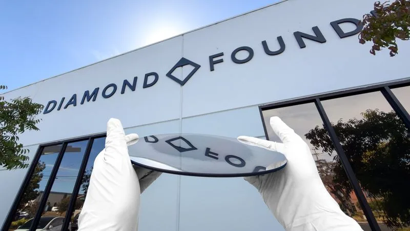
The Diamond Foundry has come out with its claim of making the world’s first 200mm continuous single crystal diamond wafer. It is a great achievement, which can have immense impact on the future of semiconductors used in artificial intelligence, high-performance computing, and power electronics. The achievement is the first time when a single crystal diamond wafer is successfully grown at the standard diameter of 200mm in use throughout the chip fabrication facilities.
The difference from polycrystalline diamond films or composites which are made from wafers formed by joining smaller wafers is that this newly manufactured wafer is made of one continuous crystal only. According to the company itself, this sample was presented in an as-grown state, which means it was not yet processed and did not undergo any kind of surface polishing. To achieve this result, about 25 years of extensive research were needed with the help of Diamond Foundry’s technology acquired from the German diamond engineer Audiatec.
The creation of the wafer involved the use of Diamond Foundry’s heteroepitaxial growth technique. In this technique, the researchers started with a silicon wafer coated with a unique template composed of iridium and a zirconium oxide layer. In the process, it became possible to induce carbon atoms in a highly ordered arrangement into a diamond crystal lattice and overcome the structural mismatch challenges that had been preventing scientists from growing large single-crystal diamonds.
It comes at the most crucial time for the semiconductor industry which faces the challenge of excessive heat accumulation in densely packed, increasingly powerful microprocessors. Indeed, Diamond has always been known as an extremely efficient thermal conductor second to none, conducting heat better and faster than copper and silicon and serving as a good insulator of electricity and a very strong material. It can be concluded that diamond substrate can help deal with current cooling problems.
With advancements in artificial intelligence accelerators and HPC (high-performance computing) chips, heat tends to concentrate in localized areas due to high density of the transistors in the chip area. This can lead to heat throttling computing and reducing the life of the hardware. According to Diamond Foundry, the idea is that one day, single crystal diamond wafers can be directly attached to the silicon circuit wafers in the vicinity of the transistor layer, thus cooling more efficiently than previous packaging materials.
An upgrade to 200 mm is quite a considerable leap compared to the 100 mm single crystal diamond wafer that Diamond Foundry first introduced in 2023. The reason behind this is due to the fact that contemporary semiconductor production facilities depend entirely on the 200mm and 300mm fabrication processes. The achievement of this target of 200mm places the diamond substrates closer to being compatible with the machinery in existing facilities.
Despite all of this, Diamond Foundry is aware of the challenges lying ahead and states that there is still several years until the technology finds widespread commercial applications. At the moment, the breakthrough revolves around one prototype wafer and not mass production. For commercial implementation of the technology by chipmakers, the engineers should increase the production yield, work on polishing the surface, create reliable methods of wafer bonding, prove the reliability, and reduce costs of manufacturing.
At the moment, the company has not announced any schedule for commercialization and future partners from the industry. Diamond Foundry is going to concentrate on improving the fabrication process and increasing yield before shipping the samples to potential customers. Although the technology of diamond cooling is becoming more and more popular in light of overheating of AI hardware, there are still many obstacles to overcome.