
Taiwan-based GaNrich Semiconductor Corporation has unveiled its comprehensive portfolio of gallium nitride (GaN) power devices spanning 40V to 1200V, establishing itself as a dedicated wide-bandgap specialist capable of dual-platform volume manufacturing. Leveraging proprietary manufacturing capabilities across both GaN-on-Silicon and GaN-on-Sapphire wafer substrates, the company provides complete voltage coverage for mission-critical power conversion. The product rollout addresses escalating global demands across artificial intelligence data center power delivery, battery backup units, industrial robotics, autonomous drones, electric vehicles, and high-voltage on-board chargers.
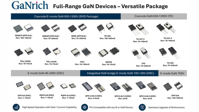
Commercial wide-bandgap deployment has traditionally remained fragmented, with most GaN vendors concentrating strictly on 650V-and-below lateral devices. GaNrich has bridged this landscape by supplying validated, mass-production solutions across both low-mid voltage (40V–250V) and high-voltage (650V–1200V) tiers. In the 40V–250V domain, the company offers compact package footprints—including 5×6, 5×3, and 3×3 millimeter form factors—designed to deliver drop-in compatibility with legacy silicon components. To accelerate adoption and streamline printed circuit board layout, GaNrich integrates dedicated gate drivers directly into the device package, eliminating external parasitic inductance and easing design-in complexity for hardware engineers.
At higher operating potentials, the 650V–1200V portfolio targets demanding AC-DC conversion and direct bus architectures feeding accelerated computing racks and electric vehicle drivetrains. Moving into applications traditionally monopolized by silicon carbide (SiC), GaNrich is developing a 1200V bidirectional switching (BDS) device. By allowing current conduction and voltage blocking in both directions, this bidirectional architecture enables single-stage power-conversion topologies, significantly cutting passive component counts, increasing voltage margins, and shrinking magnetic footprints. The portfolio is backed by full turnkey capabilities spanning photomask layout, advanced packaging, multi-chip system module integration, and reliability qualification.
Beyond device performance, GaNrich’s expansion carries profound strategic implications for international semiconductor sourcing. The global GaN supply ecosystem remains heavily concentrated within China-based manufacturing hubs. In response to growing procurement mandates from North American and European original equipment manufacturers seeking geographic diversification, GaNrich is leveraging domestic Taiwanese wafer fabrication and outsourced packaging ecosystems alongside global supply-chain partners. This coordinated model establishes an independent, resilient “non-red” supply chain for advanced compound semiconductors.
With commercial products validated across international automotive, energy storage, and industrial customer bases, GaNrich demonstrates the scalability and manufacturing readiness of wide-bandgap platforms. As power conversion architectures transition to higher frequencies and power densities, comprehensive GaN device integration delivers a viable alternative to conventional silicon and silicon carbide.