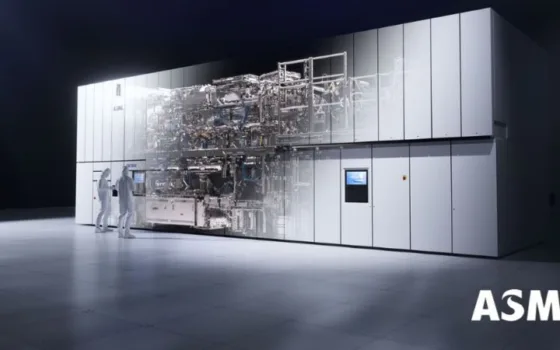
SK Telecom has deployed an industrial digital twin system across SK hynix semiconductor fabrication plants using Nvidia Omniverse, optimizing the 3D simulation platform for high-density, large-scale chipmaking environments. The implementation was officially featured during Nvidia’s GTC Taipei keynote, where SK Telecom was spotlighted as a key industrial partner in Nvidia’s global manufacturing physical AI initiative.
The collaboration supports SK hynix’s broader “Autonomous Fab 2030” roadmap. Following the completion of an initial proof-of-concept (PoC) project between SK Telecom and SK hynix last year, the companies have transitioned the technology directly into active semiconductor operations, establishing virtual replicas of operational cleanrooms and tooling infrastructure.
Agentic Modeling and High-Density Fab Simulation
Digital twin architectures recreate physical factories and wafer-processing equipment inside synchronized virtual environments. This framework allows engineers to test and validate process recipe changes, layout reconfigurations, and material handling workflows prior to executing physical changes on the cleanroom floor. By simulating operating scenarios in virtual space, fabs can suppress operational risk, reduce trial-and-error costs, and maintain tighter baseline yields.
To resolve the data bottlenecks inherent in microelectronics facilities, SK Telecom developed an “Agentic Digital Twin Modeling” technology powered by the Nvidia Agent Toolkit. This software layer automates the ingestion, parsing, and processing of heterogeneous manufacturing data:
Spatial Structuring: Converts dense plant layouts, cleanroom bays, and overhead wafer transport networks into structured 3D assets.
Automated Data Processing: Replaces labor-intensive manual conversions with autonomous scene generation and geometry optimization.
Operational Performance: Streamlines scene updates to support real-time physical AI integration across live fab floors.
Graphics and Memory Optimization for Large-Scale Scenes
Semiconductor cleanrooms present severe computational challenges for standard 3D simulation engines due to the massive volume of interrelated spatial data, piping networks, automated material handling systems (AMHS), and hundreds of processing tools.
To maintain stability under these data-intensive workloads, SK Telecom integrated specialized Nvidia Omniverse libraries directly into its platform architecture. The engineering focus centered on accelerating scene-loading speeds, boosting runtime execution performance, and maximizing both GPU and system memory utilization during large-scale 3D rendering. This optimization ensures that complex, multilayer fab models operate smoothly without latency or system crashes during real-time diagnostic simulations.
According to Mike Geyer, head of Nvidia Industrial Digital Twins, semiconductor fabs represent some of the world’s most demanding physical environments, combining massive 3D datasets, complex facility structures, and continuous optimization requirements. Geyer noted that SK Telecom successfully demonstrated the maturity of Omniverse Agent Toolkit technologies within an active industrial setting.
Cho Ik-hwan, head of Physical AI at SK Telecom, emphasized that the collaboration demonstrates how industrial AI is moving beyond basic visualization toward a comprehensive physical AI platform capable of interpreting and optimizing complex 3D manufacturing operations. The phased commercialization marks a significant milestone in transitioning memory fabs into autonomous, data-driven manufacturing plants.