
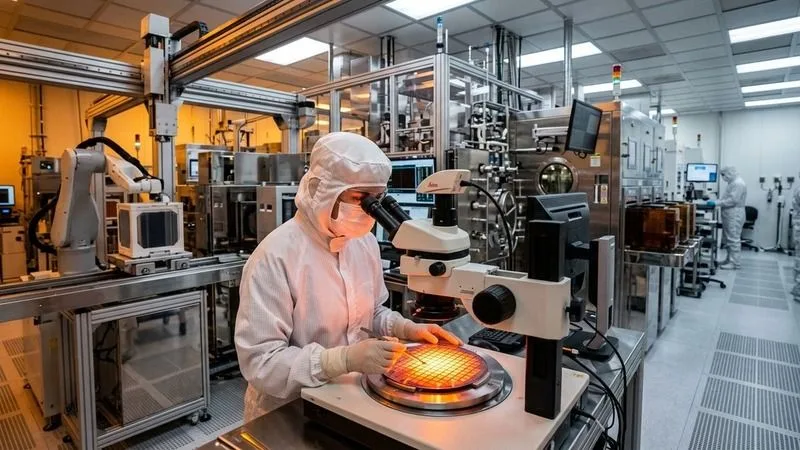
The Spintronics AI Semiconductors, a chip design and engineering company that operates from Hyderabad, has achieved an important milestone in its efforts to develop power electronics of the future. The company managed to achieve a successful wafer-out of its Gallium Nitride-on-Silicon power High Electron Mobility Transistor project. The term wafer-out in relation to chip development refers to the completion of physical manufacture of the semiconductor wafer, and the team is now ready to test how the actual device will work. The current development effort seeks to produce an ultra-high-power component of 650 volts and 20 amperes.
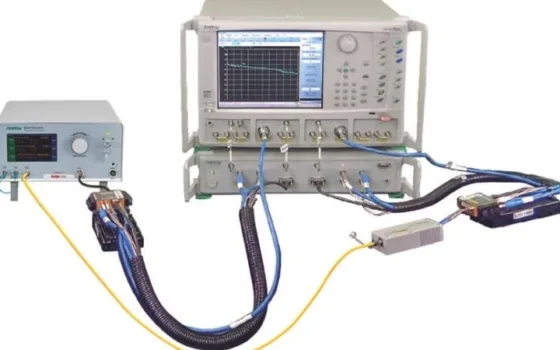
The achievement was possible thanks to the collaboration between the company and the CSIR-Central Electronics Engineering Research Institute located in Pilani. Having completed the fabrication stage, engineers can start testing the developed devices on the wafer level. The initial tests performed at the Pilani institute have yielded promising results.
The technical testing was led by senior scientist Dr. Pijus Kundu at CSIR-CEERI. As per his opinion, GaN technology has huge importance for the future of Indian chip industry in the systems with high power and high operating frequency requirement. It is a significant milestone towards developing indigenous chip technology and becoming more self-reliant in a very important part of modern electronic technologies.
GaN is considered to be a wide-bandgap semiconductor material, and due to this feature, it offers some advantages over silicon chips. The transistors based on such materials can switch the power on and off very quickly and dissipate much less heat than silicon chips. The high efficiency and power capability make such transistors excellent solutions for fast electric vehicle chargers, solar power inverters, telecommunications networks, power systems of data centers, industrial power systems, and energy storage devices. All these areas of modern technology try to put more power into small volumes without losing any energy.
According to Raghu Varma, the founder and CEO of Spintronics AI Semiconductors, a wafer-out is only possible if the right decisions have been made by an engineering team even before the actual manufacturing process starts. Varma appreciated the efforts of his engineering team and the researchers at CSIR-CEERI, stressing the fact that India has all the necessary scientific acumen and technical expertise to become a major competitor in the international power chip industry.
The collaboration between the private company and the government research institution was established via an official agreement. The collaboration brings together the more than two decades of laboratory experience in Gallium Nitride devices of CSIR-CEERI and the commercial design and product engineering capabilities of Spintronics AI. The goal of the partnership is to develop products out of advanced laboratory research.
In addition to this testing process, Spintronics AI is also exploring options to establish a manufacturing facility of Gallium Nitride chips in Ujjain, Madhya Pradesh. This factory is currently at an early planning stage and is an essential part of the company’s long-term strategy to increase local production of semiconductors within India.
After this, the engineering team will conduct extensive electrical testing and long-term reliability tests on the new wafers. Using this data, they will make improvements to the design of the device, test packaging processes, and ensure that it complies with industrial standards. Managing Director Srijith Paruchuri mentioned that along with these power chips, Spintronics AI is also making good progress in its research work on radio frequency antenna and filter modules. All these efforts are aimed at meeting India’s increasing demands for locally manufactured components for defense, aerospace, space exploration, and satellite communication industries. Upcoming test results will determine how fast these chips will enter the market.