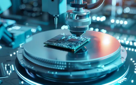

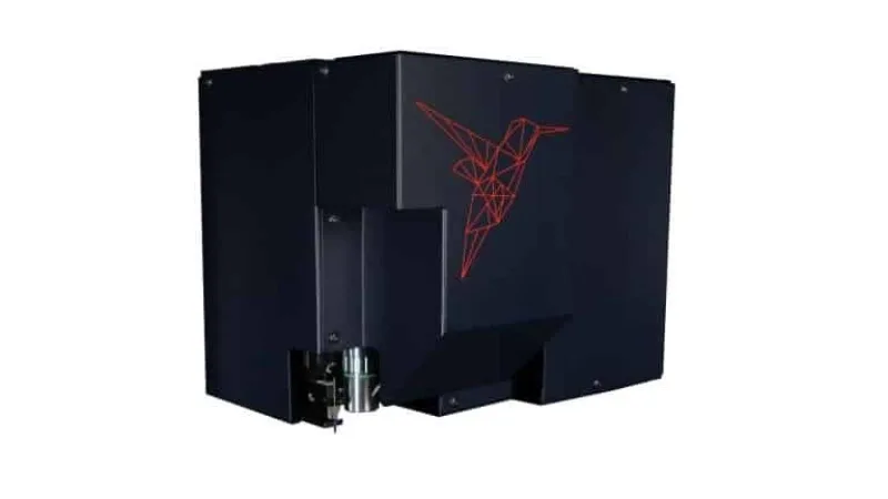
Hummink has unveiled its BIRD (Breakthrough Integration and Resolution in Defect Repair) module, introducing an industrial additive manufacturing system engineered for micron-scale printing, defect repair, and surface functionalisation across electronics production lines. Unveiled ahead of SEMICON Europa 2026 in Munich, the module integrates Hummink’s proprietary High Precision Capillary Printing (HPCaP) technology to deposit materials with resolutions spanning 0.6 to 50 micrometres. The tool addresses severe yield vulnerabilities in advanced semiconductor packaging,where open circuits and localized anomalies can cause entire multi-chip assemblies to be scrapped.
The manufacturing challenge has intensified as backend assembly migrates from traditional silicon wafers toward Fan-Out Panel-Level Packaging (FOPLP) and complex heterogeneous architectures. In high-density panel configurations, fine-pitch redistribution layers (RDLs) route critical signals between tightly spaced chiplets. However, an isolated open circuit or etching error across these microscopic metal traces historically condemned the entire large-format panel, destroying dozens of high-value dies and escalating scrap costs. Conventional inkjet printing systems lack the sub-micron resolution needed for fine-line RDL geometries, while vacuum-based thin-film deposition tools cannot deliver localized, maskless repairs.
The BIRD module circumvents these technical constraints through capillary-driven deposition. By utilizing fluidic capillary forces and mechanical resonance rather than pressurized nozzles, the printhead dispenses highly viscous conductive, dielectric, and functional inks rated up to 250,000 centipoise. This fluidic control allows operators to bridge fractured copper traces, rebuild damaged contact pads, and reconstruct missing micro-bumps directly onto glass and composite substrates without damaging adjacent circuitry. Direct, maskless material placement reduces chemical consumption, while localized post-deposition sintering rapidly cures functional lines within minutes.
The development represents a transition for HPCaP technology from laboratory demonstration into volume commercial deployment. Having established pilot runs within flat-panel and microLED display lines, Hummink is currently running production qualification trials with a major semiconductor and display fabricator in Asia. Amin M’Barki, Chief Executive Officer of Hummink, highlighted that a single RDL flaw on a panel substrate can jeopardize production for dozens of artificial intelligence processors, noting that the module provides a surgical repair mechanism that converts discarded substrates into viable production output.
For outsourced semiconductor assembly and test (OSAT) facilities and foundries scaling glass-core substrates and panel packaging, inline defect rectification provides decisive economic relief. Rescuing panels worth tens of thousands of euros mitigates backend scrap rates and lowers cost overheads across multi-chip AI hardware ecosystems. By validating additive micro-printing directly within cleanroom production lines, Hummink establishes an essential yield-recovery layer for next-generation packaging infrastructure.