The global market for Ultra-Pure Water (UPW) in semiconductor manufacturing is projected to expand from $2.16 billion in 2026 to $4.33 billion by 2035, registering a compound annual growth rate (CAGR) of 8.05%, according to a recent industrial analysis published by Business Research Insights.
This sustained market momentum is primarily propelled by the scaling of advanced semiconductor nodes to satisfy performance requirements for 5G, artificial intelligence (AI), and Internet of Things (IoT) infrastructure. As front-end device architectures become increasingly compact and complex, wafer fabs require unprecedented contamination control to prevent microscopic particulate defects from impacting device reliability and production yields.
Front-End Processing and Resistivity Requirements
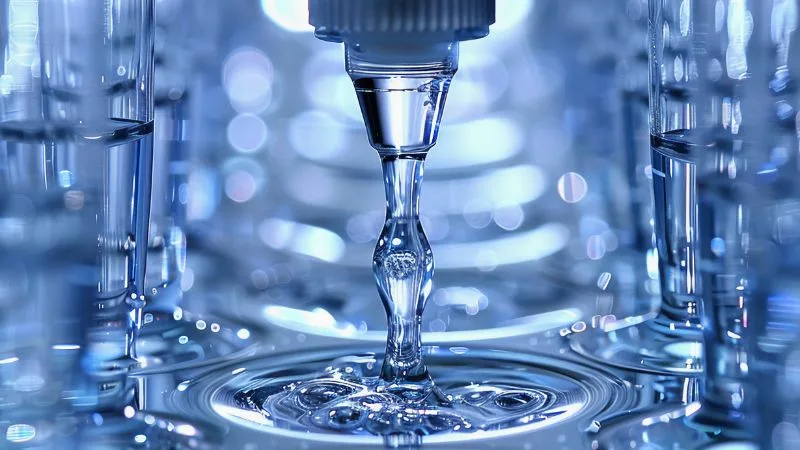
Ultra-pure water serves as a foundational utility across front-end wafer processing, functioning as an ultra-clean chemical solvent and rinsing agent. UPW is heavily utilized during silicon wafer production, wet wafer cleaning stations, and immersion lithography. Its primary technical function is to guarantee a smooth, residue-free wafer surface by stripping organic contaminants, trace ions, and microscopic particles prior to sensitive thin-film deposition, chemical etching, or thermal diffusion steps.
The market segments technically based on resistivity grades:
Resistivity 18.2 MΩ-cm : Represents the highest purity standard and commands the strongest growth. With sub-microscopic contaminants capable of inducing immediate gate dielectric breakdown or bridging defects in sub-micron processes, 18.2 MΩ-cm water has become an operational requirement for advanced-node foundries.
Resistivity 18.1 MΩ-cm: Maintains steady, consistent demand for mature node manufacturing, back-end finishing stages, and legacy wafer fabrication lines.
Smart Automation and Infrastructure Investment
To align with broader Industry 4.0 fab automation, modern UPW facility infrastructure is rapidly integrating intelligent monitoring tools. Fabs are deploying online sensors and IoT-based analytical systems to evaluate water purity in real time. This automated infrastructure facilitates predictive maintenance of membrane filtration, deionization beds, and ultraviolet treatment units, reducing unscheduled facility downtime and keeping wafer yield margins within target thresholds.
However, high capital expenditure remains a significant industry barrier. Installing multi-stage treatment equipment—including reverse osmosis, continuous electrodeionization (CEDI), degasification, and advanced analytical instrumentation—requires substantial upfront investment and elevated maintenance costs, which can challenge developing fab projects.
Regional Expansion and Key Toolmakers
From a regional perspective, Asia-Pacific remains a dominant volume consumer of UPW infrastructure, fueled by massive logic and memory fab clusters across Taiwan, South Korea, China, and Japan, alongside emerging greenfield fab projects in India and Vietnam. North America continues to lead in process R&D and technological deployment, supported by domestic fab expansions in the United States. Europe is similarly scaling its footprint, with a strong focus on water recycling efficiency and sustainable manufacturing.
Key industrial equipment and water treatment suppliers shaping the market landscape include Ovivo (Switzerland), PALL Corporation (U.S.), MKS Instruments (U.S.), Elga Labwater (U.K.), and Thermax (India). Competition among these providers focuses on improving filtration efficiency, lowering energy footprints, and scaling closed-loop reclaim systems for high-volume fabs.
Source: Business Research Insights