The global semiconductor manufacturing equipment market is projected to expand from $138.5 billion in 2025 to $273.0 billion by 2035, exhibiting a compound annual growth rate (CAGR) of 7.1%, according to an industry report published by Orion Market Research (OMR).
This multi-year expansion is being driven by continuous capacity investments by semiconductor producers seeking to meet accelerating demand across artificial intelligence (AI) computing, high-performance data centers, automotive electronics, and next-generation consumer electronics. To support these application workloads, chipmakers are ramping capital expenditures into advanced fabrication nodes, particularly sub-5nm and 3nm process technologies.
Front-End Tooling and Lithography Retain Core Demand
According to the report, the market spans both front-end and back-end supply chain stages. Front-end equipment continues to represent a core pillar of industry growth, encompassing the critical tools needed to fabricate intricate transistor structures and multi-layer device architectures on bare silicon wafers. Key front-end categories include:
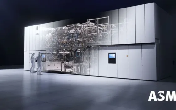
Lithography Equipment: Identified as the dominant segment by market share, lithography tooling remains foundational for patterning circuits at sub-5nm and 3nm dimensions. The market is supported by continuous advancements in extreme ultraviolet (EUV) lithography, high-throughput systems, and improved pattern accuracy.
Deposition & Etching Systems: Essential for building complex, multi-layer nanoscale architectures with high material precision.
Support Processing: Including ion implantation, chemical mechanical planarization (CMP), and wafer cleaning equipment to optimize wafer surfaces and ensure high manufacturing yield.
Key equipment suppliers have actively expanded their portfolios to match these process node transitions. For instance, Applied Materials introduced a new advanced patterning and materials engineering platform tailored to sub-3nm logic and memory production, while Lam Research expanded its portfolio of high-precision etch and deposition tools optimized for emerging 3D semiconductor architectures.
Heterogeneous Integration and Regional Capacity Expansion
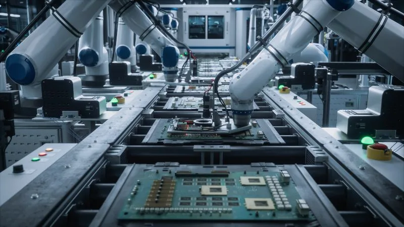
Beyond monolithic scaling, the semiconductor sector is accelerating its adoption of heterogeneous integration, 3D chip architectures, and chiplets to overcome miniaturization limits. This transition has triggered direct demand for specialized back-end assembly, bonding, wafer-level packaging, and high-precision metrology and inspection equipment capable of handling ultra-fine interconnects and multi-layer vertical configurations.
The end-user ecosystem fueling tool adoption remains led by foundries, integrated device manufacturers (IDMs), and outsourced semiconductor assembly and test (OSAT) providers, alongside research institutions.
From a geographic standpoint, the Asia-Pacific region remains the primary growth engine for equipment installations, supported by aggressive fab investments, packaging expansions, and government initiatives focused on semiconductor self-sufficiency across hubs including China, Japan, South Korea, and India. Meanwhile, North America maintains strong market standing, anchored by technology leadership, public-private funding initiatives, and cutting-edge R&D led by key global suppliers including Applied Materials, Lam Research, KLA Corporation, Tokyo Electron, and ASML.
Source: Global Research Consulting