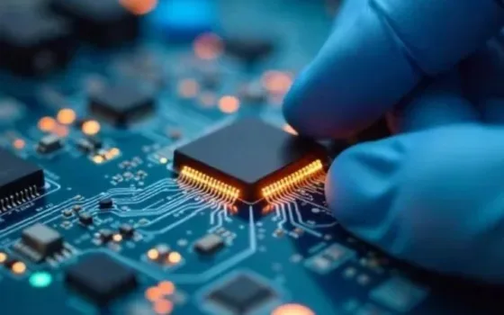

ADEKA plans to further enhance its business activities in special chemicals used for manufacture of logic integrated circuit. The semiconductor industry worldwide has witnessed the sharp rise in the demand for high-performance computing chips due to the fast adoption of artificial intelligence-based applications. Logic integrated circuit is an important component of modern-day electronics that performs crucial computation and control functions. However, due to the rapid change of chip architecture, conventional manufacturing processes do not meet requirements anymore.
Since chip producers keep improving their product line and develop increasingly complex three-dimensional structures, the process of chip manufacturing requires Atomic Layer Deposition, otherwise known as ALD. It enables applying the extremely thin and uniform layer of special material to the complex three-dimensional structures of the chip. Since there is an increasing diversity of the special ALD chemicals, as well as more complicated architectures of logic integrated circuit, the speed of introducing new products is getting increasingly important for suppliers.
Through history, ADEKA has made a good reputation for supplying ALD chemicals, especially High-k chemicals that are used in making DRAM memory chips. Using the many years of experience that ADEKA has in metal complex chemistry, ultra-high purity and strict quality control, the company is currently utilizing the same advantages in the advanced logic chip industry.
To facilitate such an expansion, ADEKA started supplying logic chip materials in 2025 from a newly established manufacturing facility in Taiwan owned by its local subsidiary company known as ADEKA FINE CHEMICAL TAIWAN CORP. The new facility is especially meant to supply new materials promptly to cater for the chip manufacturers’ testing purposes before full-scale commercial production.
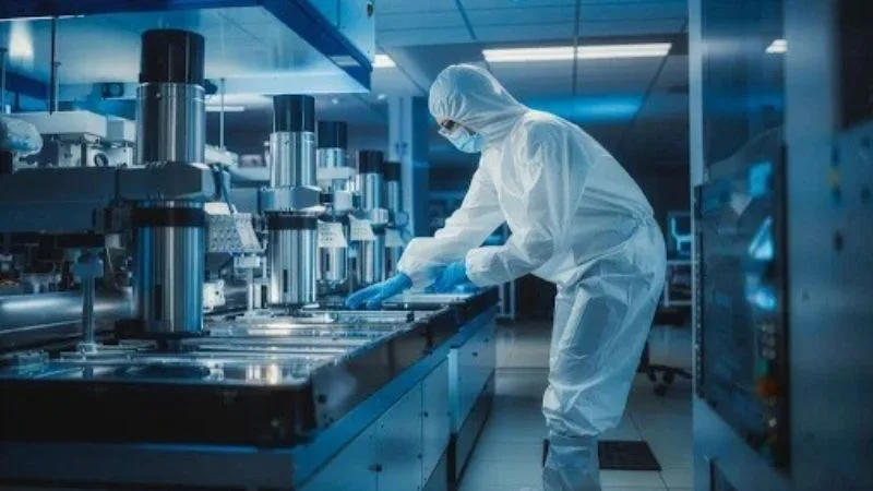
Now that the Taiwan plant is up and running, ADEKA has developed an end-to-end production pipeline that links R&D with large scale manufacturing. In this integrated process, the initial chemical research and material development are carried out at the Semiconductor Innovation Center in Kuki City, which is in the Saitama Prefecture of Japan. When the materials are ready for customer trial, small scale production and delivery is done from the Kashima Chemical Plant. At last, when the materials are ready for mass usage, the manufacturing takes place at key manufacturing locations including the newly constructed Taiwan plant.
The interconnected system enables ADEKA to adjust quickly to changes in customer timelines and increasing demands for next generation logic chips. In the future, the company will keep track of the changing market trends and customer demands and will upgrade its supply chain in a phased manner.
With its rich background in chemical engineering and its track record of reliable delivery, ADEKA is perfectly poised to take advantage of this move towards three-dimensional and smaller semiconductors. It plans on developing its logic chip materials business into a powerful engine, just like its memory chip business, and it plans on doing this in an attempt to become the leading semiconductor manufacturing materials producer in the world.