

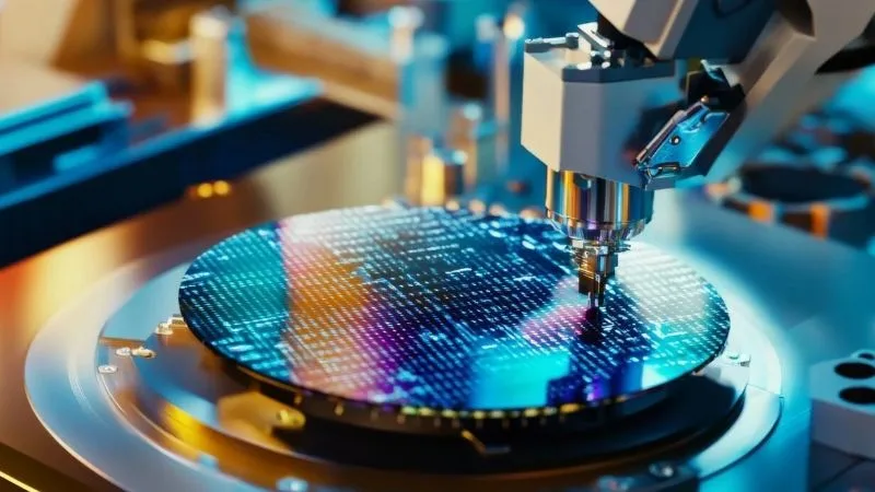
Imagine any electronic gadget from your life today: it can be a mobile phone on a table, a monitor in the dark, the dash of a modern car, or an automatic washing machine. All these gadgets will definitely have a tiny part which is a heart of the entire gadget. This part is called a microchip, an integrated circuit, or a semiconductor chip.
It might appear like a small black square of plastic or metal with some pins or solder balls on its bottom side. It might look very simple and innocent. However, this structure is one of the most sophisticated creations made by men. There could be billions of microscopic switches, called transistors, in a single chip.
Even more unbelievable is the fact that the entire process starts with something that is very common.
The process of conversion of sand into microchip is a process that takes several months and there is no disruption in the process during this period in some plants that are known as fabrication plants or “fabs”. These plants are even cleaner than the operating rooms of the hospitals and the instruments that are used in these plants operate at the scale of one million times smaller than a strand of hair. The people who make chips do not require any engineering knowledge as it is just like taking photos and painting.
Why Silicon? The Miracle Element
First of all, it should be noted that the brief analysis of silicon will be important for future discussion of the manufacturing process. Firstly, it should be noted that silicon is the second element in abundance on Earth next to oxygen. One should also note that silicon consists of quartz sand and it is mainly silicon dioxide.
There are two major groups of substances which are used for electronics. They are conductors and insulators. Conductors are those materials which ensure the free passage of electric current, copper is a good example. Insulators are those substances which do not let the electric current pass through at all, glass and rubber are good examples of these. So, one may say that silicon is a semiconductor and it is placed somehow in-between those groups of materials. In its pure form silicon is a rather bad conductor of electricity. But it is possible to make changes in its characteristics by doping.
Step 1: Wafer Preparation – from Rock / Quartz Sand to Mirror Smoothened Wafers
We start our venture with quartzite rock or superior grade quartz sand. The raw quartz sand has lots of impurities like iron, aluminum, carbon, etc. and any of these impurities may ruin the electronic circuits. To remove these impurities from quartz sand, the quartz sand is subjected to huge electric arc furnaces at 2,000°C temperature and is mixed up with carbon. Carbon reacts with oxygen in the sand and leaves behind the molten silicon with 98%-99% purity.
Now, in computer chips, 99% purity will not be useful. At this point, we require silicon of nine-nines purity, i.e., 99.9999999%. It means only one impurity atom per billion silicon atoms. To achieve this, raw silicon has to go through conversion process to silicon gas, purification by distillation several times and again converting into ultra-pure polysilicon ingots.
It is time now to make a single big crystal. The polysilicon pieces are heated in the special furnace in a quartz crucible. An engineer inserts a small pencil-shaped “seed crystal” of silicon into the liquid. While the crystal is being pulled up and rotated, the liquid silicon is cooling and creating a solid cylinder with the same atomic structure.
After several days, this process will create a big single-crystal silicon cylinder known as ingot (or boule). Modern ingots have a diameter of 300 millimeters (12 inches), weigh more than 100 kilograms and resemble shining metal cylinders.
The ingot is then polished to get the right diameter and a notch is made on the side of the ingot in order to orient the machines. With the help of highly accurate diamond-coated wires, the ingot is cut into thin discs (as if you were cutting a loaf of bread). They are silicon wafers.
Freshly sliced wafers are rough and carry microscopic saw marks. They go through chemical baths to remove surface damage and are then polished using fine slurries and rotating pads in a step called Chemical Mechanical Planarization (CMP). By the time polishing finishes, the wafer is flatter than any other man-made object on Earth, gleaming like a flawless mirror.
Step 2: Deposition – Making Microscopic Layers
And this is not the end yet. Engineers create a micro-city with many layers on the surface of the wafer. In the new generation, the chips might have more than 100 layers stacked one above another, and the thickness of each layer is less than that of a virus.
The deposition process is the method of covering the wafer with an incredibly thin layer of some specific material. There are many kinds of materials that are deposited depending on the function of a specific layer:
- Insulators (silicon dioxide or silicon nitride) are used to prevent the leakage of any electric signal between adjacent conductors.
- Conductors (copper, tungsten, aluminum) are used as small roads through which the electric charge will be transferred through the chip.
- Semiconductors (additions of silicon layers) are used as transistors’ active regions.
There are several ways factories can apply these films. In chemical vapor deposition (CVD), the wafer is put into a heated vacuum chamber where certain gases are injected. The gases undergo a chemical reaction on the heated surface of the wafer, thus forming a solid uniform film. In physical vapor deposition (PVD), a chunk of solid metal is hit by ionized gas atoms that knock off the metal’s atoms making them fall onto the wafer like very fine spray paint. The most up-to-date chips require atomic layer deposition (ALD) process, which creates the films atom by atom.
Step 3: Photolithography – The Process of “Writing” a Circuit Blueprint
After the deposition of the layer on the wafer, the next step is to etch a certain pattern onto it. Using a knife or laser to cut billions of shapes one-by-one is not possible since it would take centuries to process each wafer in such a way. So, the idea of photolithography comes into play (“writing” with light).
Firstly, the wafer is covered with a light sensitive liquid called photoresist. Then, the wafer is spun at a very high speed (thousands of revolutions per minute) to distribute the liquid evenly over the wafer surface. After that, it is baked to harden the coating.
The wafer is placed inside the lithography scanner where it is exposed to a powerful beam of light passing through a glass plate with a pattern, called a photomask (or reticle). The photomask is similar to a stencil or a negative film since it carries the pattern for one particular layer of the chip.
The light then passes through a series of very precise lenses or mirrors that reduce the image size by a factor of four and project it onto a small square on the wafer. The parts of the photoresist that are exposed to the light undergo a chemical reaction and become soft. The parts that are protected from light by the dark parts of the photomask remain hard.
The wafer is then stepped under the light beam, and the process is repeated for the entire surface of the wafer, creating a pattern of circuits on it in a grid of squares. Each square will later become an individual chip called a die. Finally, the wafer is submerged into a chemical developer that removes the soft photoresist and leaves the hardened photoresist pattern on the wafer.
Step 4: Etching and Doping — Cutting and Modifying the Silicon
Now that the photoresist is hard as a rock and protects the wafer, it is time to etch. Etching is the process of removing the exposed portions of the material below that are not protected by the photoresist stencil.
There are two main methods of etching:
- Wet Etching: The wafer is submerged in a solution that etches the exposed material. Although this technique is fast and cheap, liquids have a habit of eating sideways from underneath the stencil, which makes wet etching imprecise enough to be impractical for small structures.
- Dry Etching (also called Plasma Etching): This is the industry-standard for etching of advanced chips. The wafer is put into a chamber that is filled with some gaseous chemicals. These are excited with electricity to glow in plasma. Ions rush onto the wafer in a shower of tiny sand-blasters, cutting vertical trenches in the material below.
The Loop Continues: The 3D Skyscraper
A chip is not made in one pass only. After the first layer is deposited, printed, and etched, the wafer is immediately sent back to the start of the loop. Another layer is deposited on the wafer, covered with photoresist, exposed with another photomask, and etched once more.
In the lower layers, the engineers make billions of transistors. In the middle and upper layers, they dig trenches and fill them with copper wires which connect transistors into an enormous network – that is why these wires are called interconnects. After every cycle, the wafer is washed with ultra-pure water and flattened to provide a perfect surface for the next layer.
In a high-end processor, a single wafer passes through the loop of deposition, lithography, and etching dozens of times in three to four months. At the end, each die on the wafer turns into a multi-layer city where miles of microscopic copper wires are laid out.
Step 5: Testing and Packaging – Cutting, Testing, and Protecting
After many months of manufacturing, the wafer carries hundreds of fully functional chips organized in a grid pattern. Still, even the smallest piece of dust or an atomic imperfection can damage specific dies in the process of manufacturing. Prior to the wafer’s cutting, wafer probing occurs. In the process, an automated machine places thousands of very fine probes on the minuscule contact pads of the chip’s die and does simple testing to find out which ones work and which fail.
The next step is dicing. Either a very precise diamond blade or laser cuts along the thin “streets” dividing the squares in the wafer, separating it into individual chips. Defective dies are thrown away.
A silicon die is highly sensitive; it is fragile and may crack, corrode in humid air, and its electrical contacts are too small for soldering onto a printed circuit board. To overcome this problem, a good die undergoes packaging:
- Mounting: The chip is mounted on a rigid substrate board which consists of much larger wiring that spreads the smaller connections of the chip to wider spaces.
- Connection: Small gold or copper wires, or thousands of solder bumps, connect the electrical contacts on the silicon chip to the substrate.
- Encapsulation: The chip is encased in an insulating cover made of plastic, ceramic, or metal. In many cases, a metal cover known as the heat spreader is mounted on top of the chip in order to dissipate heat from the silicon chip during operation.
After the chip is packaged, it undergoes rigorous testing. Testing machines subject the chip to a variety of tests including electrical and performance tests, as well as temperature extremes.
The Role of Semiconductor Manufacturing Equipment
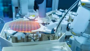
None of the above processes is possible without human hands. Actually, people working in a modern fabrication facility do not touch the wafers at all; workers have to wear full-body “bunny suits” in order not to contaminate the process with skin and hair particles, whereas wafer pods are automatically moved from one machine to another along overhead tracks.
All the work is done by special semiconductor manufacturing equipment – one of the most advanced and expensive machines ever created. All the key processes require specially designed machines provided by dedicated equipment companies:
Of all these machines, Extreme Ultraviolet (EUV) lithography scanners are perhaps the greatest inventions in contemporary technology. With a volume comparable to that of a city bus, and priced around $200 million per unit, these devices shoot powerful lasers at drops of molten tin at 50,000 pulses each second to produce extremely short wavelengths of light. This light is then reflected off the most sophisticated mirrors ever made to print lines that are only a few nanometers thick, or roughly a few silicon atom widths apart.
Just as important are metrology and inspection systems. As a matter of fact, one dust particle or a layer being even by two atoms thick enough can lead to the whole wafer batch becoming non-functional. Therefore, constant inspections during the process help to detect minor errors and tune up the whole line properly.
The process from sand to wafer to chip computing billions of operations per second is literally on the boundary between physics and engineering. Every time you touch a screen, watch a video, or start a car, you use billions of tiny switches, one of the most remarkable technical achievements of humankind.