

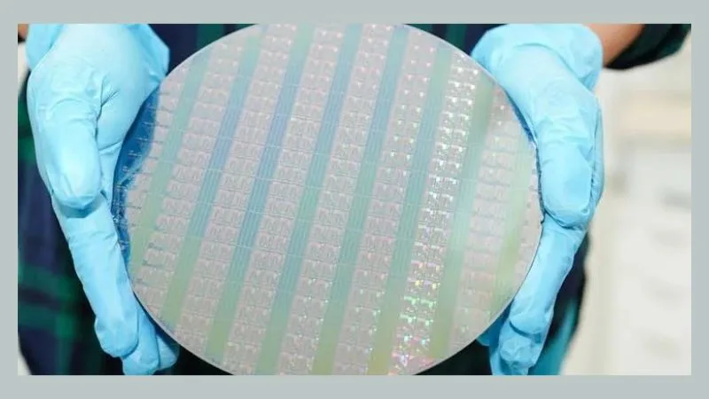
ACM Research Inc., a leading manufacturer of wafer and panel processing equipment used for semiconductor fabrication and advanced packaging, has opened its new research and development center in Hillsboro, Oregon. This opening marks a significant milestone in the first step of ACM’s strategy to invest more than 100 million dollars in its American facilities. With this expansion, ACM is set to consolidate its position as a leading equipment supplier for the world’s best chipmakers.
Covering a total area of 40,000 square feet, the new Hillsboro facility includes a 24,000-square foot manufacturing space along with a special demonstration lab for customers. By bringing together equipment assembly, engineering development, and product testing within one roof, the company has succeeded in making its home base in one place. This arrangement is meant to facilitate technology development, machinery manufacturing, and more interaction with the customers in North America.
For ACM, a company based in Silicon Valley, since the year 1998, its image was created through the development of semiconductor process technology that has made it into a reliable equipment supplier on a global scale. The establishment of the Oregon plant is an important milestone towards the company’s strategy of strengthening its home base foundation and at the same time, developing its manufacturing capacity on the international front. Through building its local engineering and assembly workforce, ACM aims to operate shoulder to shoulder with the American chip makers.
This means that the client located in North America will have easy access to the facilities provided by ACM and will be able to use the advanced wafer and panel processing equipment. The clients will be able to go to the demonstration lab to test the wet cleaning and electrochemical plating equipment used for front-end wafer fabrication and advanced packaging. At the same time, placing all researchers, manufacturers, and customer support specialists in one place will allow engineers to get real-world feedback and improve their equipment in terms of reliability and performance.
The expansion will not only improve the manufacturing process but will also improve customer service in the region. As ACM will get more parts and a bigger technical support team, it will be able to respond faster to the maintenance requests and decrease equipment downtime in the nearby fabrication plants.
Oregon has been an important hub for ACM’s domestic operations from the day the company set up its sales and service office in Hillsboro in 2023. The new facility is a direct continuation of ACM’s presence in Oregon’s renowned Silicon Forest semiconductors area. Located amidst a host of leading semiconductor producers, engineers, and component suppliers, the Hillsboro site provides ACM with a solid platform to enhance its position in the American semiconductor industry value chain.